Encapsulation structure for OLED device and encapsulation method and lighting device of OLED device

A packaging structure and packaging method technology, which is applied in semiconductor devices, electrical solid devices, semiconductor/solid device manufacturing, etc., can solve problems such as peeling off, low elasticity of inorganic films, and poor water and oxygen barrier capabilities

Inactive Publication Date: 2014-06-25
BOE TECH GRP CO LTD +1
View PDF13 Cites 38 Cited by
  • Summary
  • Abstract
  • Description
  • Claims
  • Application Information

AI Technical Summary

Problems solved by technology

[0004] In substrate encapsulation, since the adhesive film is usually an organic binder, a large number of pores will be produced after curing, so that water and oxygen in the air can react with OLED devices through these pores; in thin film encapsulation, although the inorganic thin film is dense However, during the preparation process of the inorganic film, defects such as pinholes and cracks will inevitably appear, which greatly reduce the ability of the inorganic film to isolate water and oxygen, and the inorganic film The elasticity is low, the internal stress is large, and it is easy to crack or peel off from the OLED device under the action of external force. Therefore, it needs to be laminated with an organic film to form a composite film, but the organic film has poor barrier ability to water and oxygen, and even some organic films The material itself has strong water absorption, so that water vapor has the opportunity to enter the interior of the OLED device through the defects of the adjacent inorganic film.

Method used


Image

  • Encapsulation structure for OLED device and encapsulation method and lighting device of OLED device
  • Encapsulation structure for OLED device and encapsulation method and lighting device of OLED device
  • Encapsulation structure for OLED device and encapsulation method and lighting device of OLED device

Examples


Embodiment Construction

[0031] The technical solutions in the embodiments of the present invention will be clearly and completely described below in conjunction with the accompanying drawings in the embodiments of the present invention. Obviously, the described embodiments are only a part of the embodiments of the present invention, rather than all the embodiments. Based on the embodiments of the present invention, all other embodiments obtained by those of ordinary skill in the art without creative work shall fall within the protection scope of the present invention.

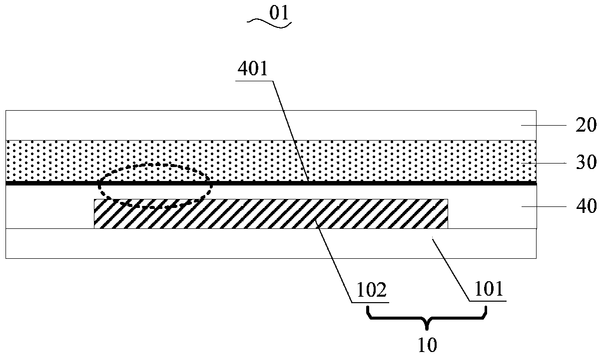
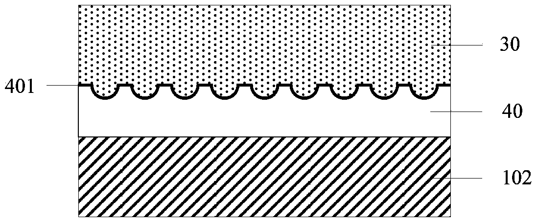
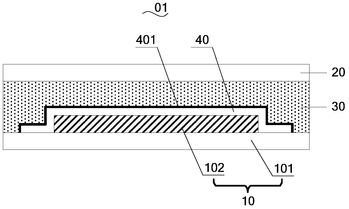
[0032] The embodiment of the present invention provides an OLED device packaging structure 01, such as Figure 1 ~ Figure 3 As shown, the packaging structure 01 includes: a device substrate 10, a packaging substrate 20 that is boxed with the device substrate 10, and an adhesive film 30 between the device substrate 10 and the packaging substrate 20. The device The substrate 10 includes a base substrate 101 and an OLED device 102 located o...


PUM


Abstract

The embodiment of the invention relates to the field of encapsulation manufacture of OLED devices and provides an encapsulation structure for an OLED device and an encapsulation method and a lighting device of the OLED device. The combining strength between an adhesive film and a buffer layer in the encapsulation structure of the OLED device can be increased, the probability that water oxygen invades the OLED device between the adhesive film and the buffer layer is reduced, and the encapsulation effect of the OLED device is improved. The encapsulation structure comprises a device substrate, an encapsulation substrate forming a box with the device substrate and the adhesive film located between the device substrate and the encapsulation substrate, and the device substrate comprises a substrate body and the OLED device located on the substrate body. The encapsulation device further comprises the buffer layer located between the device substrate and the adhesive film, wherein one side, in contact with the adhesive film, of the buffer layer is provided with an uneven surface. The encapsulation structure for the OLED device is applied to encapsulation manufacturing of the lighting device comprising the encapsulation structure.

Description

Technical field [0001] The invention relates to the field of packaging and preparation of OLED devices, in particular to an OLED device packaging structure, a packaging method thereof, and a light emitting device. Background technique [0002] The OLED devices in Organic Light-Emitting Diode (OLED) easily react with water vapor, oxygen and other components in the air. Therefore, they need to be strictly separated from the water and oxygen in the environment to extend the Service life. [0003] Traditional packaging methods include substrate packaging and thin film packaging. Among them: substrate packaging refers to filling an adhesive film between the device substrate on which the OLED device is formed and the packaging substrate. After the adhesive film is cured, the device substrate and the packaging substrate are formed A closed space to achieve the encapsulation effect; thin-film encapsulation refers to covering the surface of the OLED device with a thin-film encapsulation la...

Claims


Application Information

Patent Timeline
Patent Type & Authority Applications(China)
IPC IPC(8): H01L51/52H01L51/56
CPCH10K50/84H10K71/00H10K50/844H10K50/858H10K50/8426
Inventor 全威王俊然
Owner BOE TECH GRP CO LTD
Why Eureka
Try Eureka