Circuit board having embedded components and manufacturing method thereof

一种内埋元件、电路板的技术,应用在非印制电元件相联接的印刷电路、用电元件组装印刷电路、印刷电路制造等方向,能够解决对位精度不佳、生产成本高等问题,达到节省成本、避免对位问题的效果

Active Publication Date: 2014-07-02
礼鼎半导体科技秦皇岛有限公司 +1
View PDF5 Cites 26 Cited by
  • Summary
  • Abstract
  • Description
  • Claims
  • Application Information

AI Technical Summary

Problems solved by technology

[0005] In the above-mentioned manufacturing method of a circuit board with embedded components, the electronic components are first fixed on the supporting material layer and embedded, and then conductive blind holes are formed for electrical connection, and the alignment accuracy between the conductive blind holes and the electronic components is likely to be poor.
Especially in the production of large boards, when electronic components are placed, a high-precision placement machine is required, and the production cost is high

Method used


Image

  • Circuit board having embedded components and manufacturing method thereof
  • Circuit board having embedded components and manufacturing method thereof
  • Circuit board having embedded components and manufacturing method thereof

Examples


Embodiment Construction

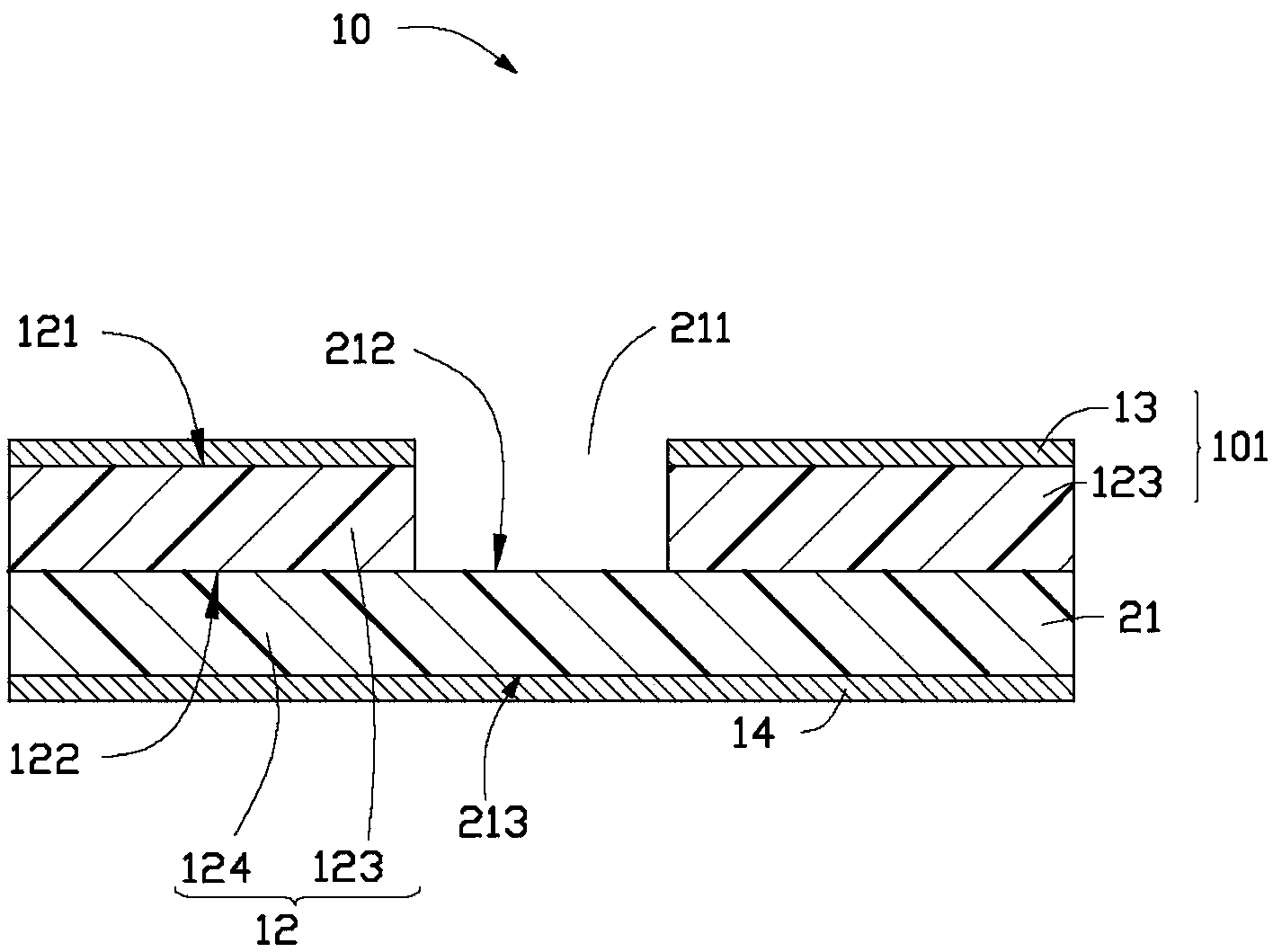
[0020] see Figures 1 to 8 , an embodiment of the present invention provides a method for manufacturing a circuit board with embedded components, comprising the following steps:

[0021] Step 1: See figure 1 The single-sided copper clad substrate 101 having the opening 211 , the first insulating layer 124 and the second copper foil layer 14 are sequentially stacked and pressed together at one time to form a double-sided copper clad substrate 10 .

[0022] The single-sided copper-clad substrate 101 includes a base material layer 123 and a first copper foil layer 13, the base material layer 123 includes opposite first surfaces 121 and second surfaces 122, and the first copper foil layer 13 is disposed on the base material layer 123 of the first surface 121 . The material of the first insulating layer 124 is generally a film, such as FR4 epoxy glass cloth prepreg, and the first insulating layer 124 includes a third surface 212 and a fourth surface 213 opposite to each other. T...


PUM


Abstract

A printed circuit board with an embedded component includes a double-sided wiring board, an electronic component, and many conductive pastes. The wiring board includes a first wiring layer, a base layer, a first insulating layer, and a second wiring layer. The base layer has an opening exposing a portion of the second surface of the first insulating layer to the outside. The second wiring layer includes electrical contact pads. The conductive blind vias are formed in the first insulating layer. Each electrical contact pad is electrically connected to an end of the corresponding conductive blind via. The other ends of the conductive blind vias are adjacent to the first surface. A filling through hole is formed in the double-sided wiring board. The conductive pastes are respectively electrically connected to the conductive blind vias. The electronic component is adhered to and electrically connected to the conductive paste.

Description

technical field [0001] The invention relates to the field of circuit board production, in particular to a circuit board with embedded components and a production method thereof. Background technique [0002] Printed circuit boards have been widely used due to their advantages such as high assembly density. For the application of the circuit board, please refer to the literature Takahashi, A. Ooki, N. Nagai, A. Akahoshi, H. Mukoh, A. Wajima, M. Res. Lab, High density multilayer printed circuit board for HITAC M-880, IEEE Trans . on Components, Packaging, and Manufacturing Technology, 1992, 15(4): 1418-1425. [0003] In order to achieve the purpose of light, thin and short, and increase the electrical quality level of the multilayer circuit board in the prior art, various manufacturers have begun to devote themselves to changing the electronic components that were originally soldered on the surface of the multilayer circuit board to be embedded in the multilayer circuit board...

Claims


Application Information

Patent Timeline
Patent Type & Authority Applications(China)
IPC IPC(8): H05K3/32H05K3/42H05K1/18
CPCH05K1/113H05K3/32H05K1/183H05K1/115H05K1/186H05K3/4602H05K2201/09072H05K2201/10636Y10T29/4913H05K3/4697Y02P70/50
Inventor 许诗滨
Owner 礼鼎半导体科技秦皇岛有限公司
Why Eureka
Try Eureka