Solder joint quality inspection method of stacked package device

A technology of stack packaging and solder joint quality, applied in the direction of optical testing flaws/defects, etc., can solve the problems of unresponsive solder joint cracking, long inspection cycle, complicated operation, etc., achieving low cost, short inspection cycle, and operability. strong effect

Active Publication Date: 2016-02-17
FIFTH ELECTRONICS RES INST OF MINIST OF IND & INFORMATION TECH
View PDF6 Cites 0 Cited by
  • Summary
  • Abstract
  • Description
  • Claims
  • Application Information

AI Technical Summary

Problems solved by technology

However, metallographic sections can only observe one row of solder joints at a time, the detection cycle is longer, and the operation is more complicated
However, X-ray inspection often cannot reflect defects such as solder joint cracking, and the accuracy is low

Method used


Image

  • Solder joint quality inspection method of stacked package device
  • Solder joint quality inspection method of stacked package device
  • Solder joint quality inspection method of stacked package device

Examples


Embodiment Construction

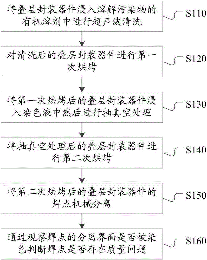
[0029] The specific implementation of the method for inspecting the solder joint quality of package-on-package devices according to the present invention will be described in detail below in conjunction with the accompanying drawings.

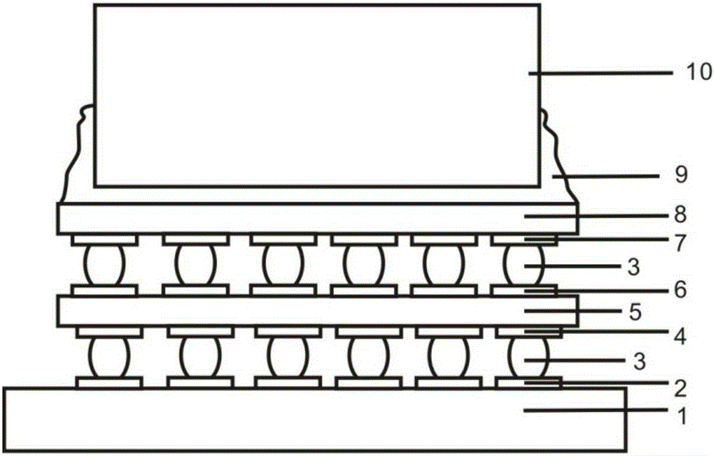
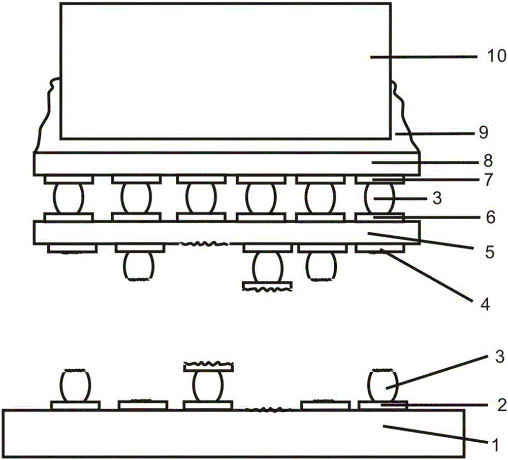
[0030] Such as figure 1 As shown, a method for inspecting the quality of solder joints of package-on-package devices includes steps:

[0031] S110, immersing the stacked packaging device in an organic solvent that dissolves pollutants for ultrasonic cleaning, so as to clean away the pollutants of the stacked packaging device, so as to avoid affecting subsequent detection results;

[0032] S120. Baking the cleaned stack package device for the first time, so as to dry the organic solvent;

[0033] S130. Immerse the stacked packaging device after the first baking in the dyeing solution, and then perform a vacuum treatment, and remove the air bubbles in the stacked packaging device through the vacuuming treatment, so that the dyeing solution is fu...


PUM


Abstract

The invention provides a quality test method for the welding spots of a PoP device. The quality test method comprises the following steps: immersing the PoP device in an organic solvent capable of dissolving pollutants for ultrasonic cleaning; subjecting the cleaned PoP device to primary baking; immersing the PoP device having undergone primary baking in a staining solution and then carrying out vacuum-pumping; subjecting the PoP device having undergone vacuum-pumping to secondary baking; subjecting the welding spots of the PoP device having undergone secondary baking to mechanical separation; and observing whether the separation interfaces of the welding spots are stained to determine whether there is a quality problem. The method can be carried out at normal temperature and normal pressure and has low requirements on equipment, strong operationality and low cost; since a plurality of rows of welding spots can be observed at the same time, so a test period is short; test results realize overall and rapid reflection of welding quality of welding spots of the PoP device.

Description

technical field [0001] The invention relates to the technical field of stacked packaging devices, in particular to a method for inspecting the quality of solder joints of stacked packaging devices. Background technique [0002] At present, the rapid development of portable electronic devices such as smartphones, notebook computers, and digital cameras has put forward higher requirements for microelectronic packaging, pushing it towards miniaturization, high reliability, and low power consumption. Package on Package (PoP) is an advanced packaging technology emerging in the process of miniaturization of modern microelectronic packaging. This technology was first introduced by Amkor. [0003] PoP devices generally refer to a new package that is formed by superimposing another corresponding package on a bottom package. During the electronic assembly process, the biggest risk PoP devices face is warpage, which can lead to cracking of solder joints, failures such as pillows (Head...

Claims


Application Information

Patent Timeline
Patent Type & Authority Patents(China)
IPC IPC(8): G01N21/91
Inventor 李伟明邹雅冰肖慧梁朝辉许慧
Owner FIFTH ELECTRONICS RES INST OF MINIST OF IND & INFORMATION TECH
Why Eureka
Try Eureka