Method for soldering element in deep-cavity small hole of printed board

A printed board and soldering technology, applied in the direction of assembling printed circuits with electrical components, can solve the problems of inability to achieve special structural forms of welding, difficult to evaluate welding effects, and limited component welding methods, to achieve welding automation, improve Solder joint quality consistency and the effect of improving welding efficiency

Pending Publication Date: 2021-04-16
BEIJING RES INST OF TELEMETRY +2
View PDF0 Cites 0 Cited by
  • Summary
  • Abstract
  • Description
  • Claims
  • Application Information

AI Technical Summary

Problems solved by technology

[0004] The technical problem of the present invention is: the purpose is to overcome the above-mentioned defects of the traditional reflow soldering technology, and provide a method for soldering components in the small hole of the deep cavity of the printed board. The present invention uses laser soldering technology to successfully realize multiple The high-reliability welding of components in the deep cavity and small hole of the multi-layer printed board solves the welding problem of special structural forms that cannot be realized by traditional processes
Due to the special structural characteristics of the printed board of the product, to realize the welding of the components and the printed board in the small hole of the deep cavity, the invention uses the laser soldering technology, adopts the method of preheating the welded and adjusting the laser process parameters, and successfully The welding of components in this type of structure has been realized, and the quality of solder joints has been characterized by a series of testing methods, which solves the problem of limited welding methods for components in small holes in deep cavities of printed boards and difficult evaluation of welding effects. The application of more electronic products has great reference and guiding significance

Method used


Image

  • Method for soldering element in deep-cavity small hole of printed board
  • Method for soldering element in deep-cavity small hole of printed board
  • Method for soldering element in deep-cavity small hole of printed board

Examples


Embodiment 1

[0036] Adopt the welding method designed by the present invention, that is: drop Sn63Pb37 solder containing flux into the small hole of the deep cavity of the printed board, and adopt the method of laser soldering to carry out element welding. The number of test pieces is 3, such as Figure 4 Shown, numbered A01~A03.

[0037] 1. Basic conditions

[0038] (1) Printed board

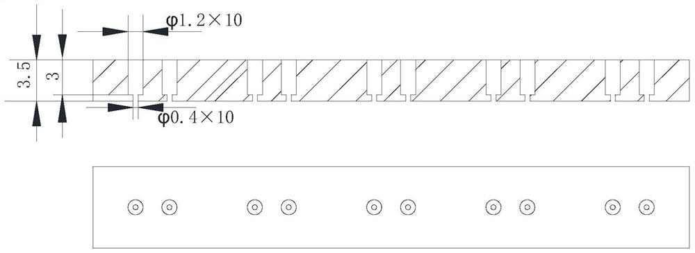
[0039] The printed board of this embodiment. In order to effectively verify the welding quality of components, the printed board design strives to be simplified to avoid introducing other factors. Printed board structure such as figure 1 , the material is Rogers4350B, the thickness is 3.5mm, a total of 4 layers, of which the pad is set on the third layer, the hole diameter is 1.2mm, the depth is 3mm, and each board is equipped with 10 deep hole pads;

[0040] (2) Components

[0041] Electrical connector JM2018-3

[0042] (3) Solder and flux

[0043] The solder selection surface is coated with R-type...

Embodiment 2

[0078] Adopt the welding method designed by the present invention, that is: drop Sn63Pb37 solder containing flux into the small hole of the deep cavity of the printed board, and adopt the method of laser soldering to carry out element welding. The number of test pieces is 3 pieces, numbered B01~B03.

[0079] 1. Basic conditions

[0080] (1) Printed board

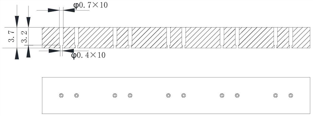
[0081] Printed board structure such as figure 2 , the material is Rogers5880, the thickness is 3.7mm, and there are 5 layers in total. The pads are set on the fourth layer, the hole diameter is 0.7mm, and the depth is 3.2mm. There are 10 deep hole pads per board.

[0082] (2) Components

[0083] Same as "Example 1".

[0084] (3) Solder and flux

[0085] The solder is selected to contain R-type flux Sn63Pb37 solder balls, and the diameter of the solder balls is 0.5mm

[0086] (4) Production and testing tools and equipment

[0087] Same as "Example 1".

[0088] Two, process implementation steps

[0089] Step (1), pro...

Embodiment 3

[0107] Adopt the welding method designed by the present invention, that is: put the solder containing flux Sn63Pb37 into the small hole of the deep cavity of the printed board, and use the method of laser soldering to weld the components. The number of test pieces is 5 pieces, numbered C01~C05.

[0108] 1. Basic conditions

[0109] (1) Printed board

[0110] The material of the printed board is FR-4, the thickness is 3.5mm, and there are 5 layers in total. The pad is set on the fourth layer, the hole diameter is 1.2mm, and the depth is 3.0mm.

[0111] (2) Components

[0112] J119A series electrical connector (10-pin).

[0113] (3) Solder and flux

[0114] The solder is made of Sn63Pb37 solder wire containing RMA flux, the diameter of the wire is 0.38mm, and the winding wire is a welding ring with an outer diameter of 1mm.

[0115] (4) Production and testing tools and equipment

[0116] Same as "Example 1".

[0117] Two, process implementation steps

[0118] Step (1), p...


PUM

PropertyMeasurementUnit
diameteraaaaaaaaaa
thicknessaaaaaaaaaa
thicknessaaaaaaaaaa

Abstract

The invention relates to a method for soldering an element in a deep-cavity small hole of a printed board, belongs to the technical field of earth electronic assembly, and particularly relates to a method for realizing high-reliability soldering of the element in the deep-cavity small hole of the printed board, wherein the diameter of the deep-cavity small hole is 0.5-2mm, and the radius-depth ratio is less than or equal to 0.5. According to the method, the welding method of laser soldering is adopted, the local, deep-cavity and small-hole welding requirements which cannot be met by traditional welding methods such as wave soldering and reflow soldering are met, and welding of elements in deep-cavity small holes with the diameter ranging from 0.5 mm to 2 mm and the diameter-depth ratio being less than or equal to 0.5 is successfully achieved by adjusting technological parameters. Inspection data such as appearance microscopic inspection, electrical property test, X-Ray nondestructive test and weld microstructure analysis after an experiment show that welding spots formed according to the welding method are good in quality.

Description

technical field [0001] The invention relates to a method for soldering components in a small hole in a deep cavity of a printed board, which belongs to the field of electronic assembly technology, in particular to a method for realizing high-reliability soldering of components in a small hole in a deep cavity of a printed board In the welding method, the small hole in the deep cavity refers to a small hole with a diameter of 0.5-2mm and a diameter-to-depth ratio of ≤0.5. Background technique [0002] With the advancement of electronic technology, the packaging of electronic components used is developing in the direction of "miniaturization", "high density" and "fine pitch". Microelectronics technology includes microelectronic components and microelectronic assembly (connection) technology. So far, the main factor that restricts the further realization of high performance and miniaturization of electronic products is no longer the components themselves, but the assembly meth...

Claims


Application Information

Patent Timeline
Patent Type & Authority Applications(China)
IPC IPC(8): H05K3/32H05K3/34
Inventor 武素星赵志勇林玉婕于溪廖声冲李建华曾令迪
Owner BEIJING RES INST OF TELEMETRY
Why Eureka
Try Eureka