TFT array substrate, liquid crystal display panel and liquid crystal display

A technology of array substrates and substrates, applied in instruments, nonlinear optics, optics, etc., can solve the problems that liquid crystals cannot be rotated, cannot pass through, and change the polarization direction of linearly polarized light, so as to improve light transmittance, improve display performance, reduce small area effect

Active Publication Date: 2014-07-23
XIAMEN TIANMA MICRO ELECTRONICS +1
View PDF7 Cites 15 Cited by
  • Summary
  • Abstract
  • Description
  • Claims
  • Application Information

AI Technical Summary

Problems solved by technology

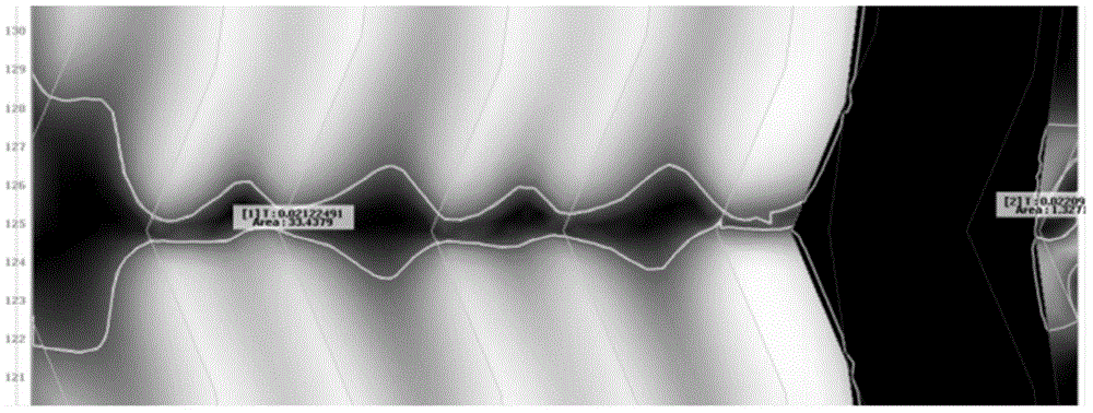
[0004] Although the existing dual-domain structure can improve the viewing angle, there is a defect: at the junction of the two domains in the pixel area, such as figure 1 At the position indicated by the reference numeral 12, the liquid crystal cannot rotate due to the electric field formed by the pixel electrodes in the two domain regions in the vertical direction with the same magnitude and opposite direction, so the liquid crystal cannot rotate. Therefore, the position indicated by the reference numeral 12 The liquid crystal cannot play the role of changing the polarization direction of the linearly polarized light, and eventually the light source cannot pass through the upper polarizer at all gray levels except the zero-level gray level, that is, at the position indicated by reference numeral 12 will produce a black line
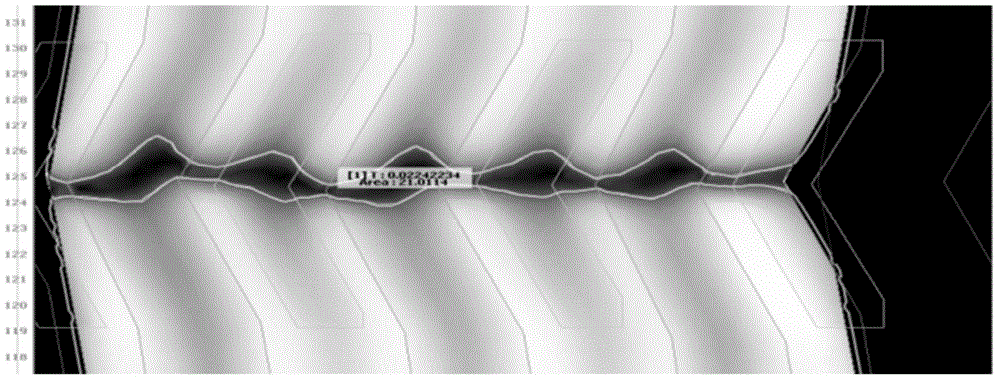
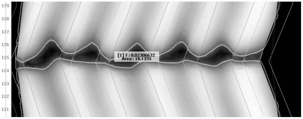
exist figure 2 shows the disclination phenomenon of the existing dual-domain pixel region, such as figure 2 As shown, the junction region of the two domain regions has a certain area of ​​black region (dislocation region), and the light transmittance of the liquid crystal display decreases

Method used


Image

  • TFT array substrate, liquid crystal display panel and liquid crystal display
  • TFT array substrate, liquid crystal display panel and liquid crystal display
  • TFT array substrate, liquid crystal display panel and liquid crystal display

Examples


no. 1 example

[0052] Figure 6 It is a schematic diagram of the TFT array substrate based on the FFS dual-domain structure according to the first embodiment of the present invention. Such as Figure 6 As shown, the TFT array substrate includes: a substrate 61; a plurality of scanning lines 62 and a plurality of data lines 63 located on the substrate 61, and the plurality of scanning lines 62 and the plurality of data lines 63 intersect to form a plurality of 64 pixel areas.

[0053] Among them, in Figure 7A A schematic structural diagram of a pixel region of a TFT array substrate according to the first embodiment of the present invention is shown in .

[0054] exist Figure 7A shows a schematic structural diagram of a pixel region of a TFT array substrate when the pixel electrodes and compensation electrodes in the pixel region are regular strip-shaped electrodes.

[0055] Such as Figure 7A As shown, each pixel region 64 includes a plurality of pixel electrodes 641 located in the pi...

no. 2 example

[0073] In this embodiment, the TFT array substrate is an array substrate based on an IPS dual-domain structure, wherein the array substrate of this embodiment includes:

[0074] Substrate;

[0075] A plurality of scanning lines and a plurality of data lines located on the substrate, a plurality of pixel areas defined by intersections of the plurality of scanning lines and the plurality of data lines;

[0076] Among them, in Figure 9A is a schematic structural diagram of the pixel region of the array substrate based on the IPS dual-domain structure when the pixel electrodes and the compensation electrodes in the pixel region are regular strip electrodes in the second embodiment of the present invention.

[0077] Such as Figure 9A As shown, each pixel area includes:

[0078] A plurality of pixel electrodes 91 and a plurality of common electrodes 92 located in the pixel area, each pixel electrode 91 and each common electrode 92 are in the shape of bent strips and arranged in...


PUM


Abstract

The invention discloses a TFT array substrate, a liquid crystal display panel and a liquid crystal display. The TFT array substrate comprises a plurality of pixel electrodes, a first insulating layer and a plurality of compensation electrodes. The pixel electrodes are located in a pixel area, the pixel electrodes are in a bent strip shape and are arranged at intervals, the pixel area is divided into two domain areas by bending portions of the pixel electrodes, the first insulating layer is arranged on the pixel electrodes, the compensation electrodes are arranged on the first insulating layer and are arranged between the pixel electrodes, each compensating electrode is arranged between every two pixel electrodes, the compensating electrodes are in a bent strip shape, and the bending portions of the compensation electrodes are located at the connecting position of the two domain areas. According to the TFT array substrate, the liquid crystal display panel and the liquid crystal display, the area of the disclination area in a double-domain structure of the IPS and FFS mode is reduced, the display performance of the double-domain structure is improved, and the light penetration rate of the liquid crystal display is improved.

Description

technical field [0001] The present invention relates to the field of liquid crystal display technology, in particular to the field of array substrate structure technology, in particular to a TFT array substrate, a liquid crystal display panel and a liquid crystal display. Background technique [0002] IPS (In-Plane Switching, in-plane switching) mode and FFS (Fringe Field Switching, fringe field switching) mode liquid crystal display provide a liquid crystal device structure with a wide viewing angle, and the pixel electrode and the common electrode are arranged on the same substrate. The liquid crystal is driven by generating a transverse electric field force to change the orientation angle of the optical axis of the liquid crystal molecules in a plane parallel to the substrate. Among them, the single domain (one domain) technology in IPS and FFS modes is widely used due to its advantages of wide viewing angle, small color shift, and low power consumption. However, as user...

Claims


Application Information

Patent Timeline
Patent Type & Authority Applications(China)
IPC IPC(8): G02F1/1362G02F1/1368G02F1/1343
Inventor 张志坚
Owner XIAMEN TIANMA MICRO ELECTRONICS
Why Eureka
Try Eureka