High-speed global shutter image sensor pixel and its pixel signal acquisition method
An image sensor, global shutter technology, applied in image communication, TV, color TV components, etc., to achieve the effect of reducing frame transfer time
- Summary
- Abstract
- Description
- Claims
- Application Information
AI Technical Summary
Problems solved by technology
Method used
Image
Examples
Embodiment 1
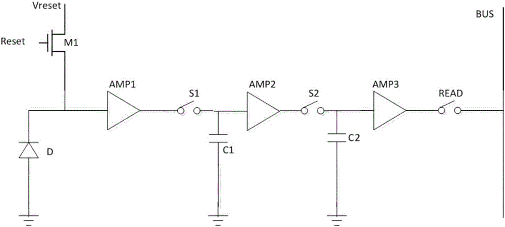
[0036] Such as Figure 4 As shown, the high-speed global shutter image sensor pixel of the present invention includes a reset switch M1, a photodiode D, first and second sampling capacitors C11 and C12, first, second and third buffer amplifiers AMP1, AMP2 and AMP3, the first , the second sampling switch S1, S2, the row selection switch READ; the first buffer amplifier AMP1 is composed of the first source follower M12 and its current source load M13, and the second buffer amplifier AMP2 is composed of the second source follower M15 And its current source load M16 constitutes. The reset switch M1, the first source follower M12 and its current source load M13, the second source follower M15 and its current source load M16 all use field effect transistors; the drain of the reset switch M1 is connected to the reset voltage Vreset, The source is connected to the cathode of the photodiode D and the gate of the first source follower M12; the drain of the first source follower M12 is ...
Embodiment 2
[0046] Such as Figure 7 As shown, the high-speed global shutter image sensor pixel of the present invention includes a reset switch M1, a photodiode D, first and second sampling capacitors C11 and C12, first, second and third buffer amplifiers AMP1, AMP2 and AMP3, the first , the second sampling switches S1 and S2, and the row selection switch READ; the first buffer amplifier AMP1 is composed of a first source follower M12, and the second buffer amplifier AMP2 is composed of a second source follower M15. The reset switch M1, the first source follower M12, and the second source follower M15 all use field effect transistors; the drain of the reset switch M1 is connected to the reset voltage Vreset, and the source is connected to the cathode of the photodiode D and the first The gate of the source follower M12; the drain of the first source follower M12 is connected to the power supply voltage Vsf_pulse1, and the source is connected to the first sampling capacitor C11 and the ga...
PUM
 Abstract
Description
Claims
Application Information


