Array substrate, manufacturing method thereof, and display device

An array substrate and substrate substrate technology, applied in semiconductor/solid-state device manufacturing, optics, instruments, etc., can solve the problem of large touch blind area, improve touch performance, eliminate touch blind area, and simplify the number of film layers. Effect

Active Publication Date: 2017-02-15
BOE TECH GRP CO LTD +1
View PDF3 Cites 0 Cited by
  • Summary
  • Abstract
  • Description
  • Claims
  • Application Information

AI Technical Summary

Problems solved by technology

[0008] Embodiments of the present invention provide an array substrate, a manufacturing method thereof, and a display device, so as to solve the problem in the prior art that the touch blind area in the self-capacitance touch structure is too large

Method used


Image

  • Array substrate, manufacturing method thereof, and display device
  • Array substrate, manufacturing method thereof, and display device
  • Array substrate, manufacturing method thereof, and display device

Examples


Embodiment 1

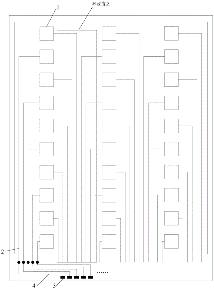
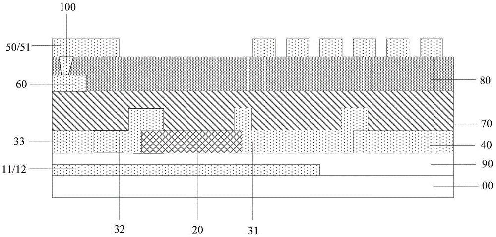
[0125] In Embodiment 1 of the present invention, the production such as figure 2 The method shown for arraying substrates is described in detail.

[0126] Preferably, the manufacturing method of the array substrate in the embodiment of the present invention includes:

[0127] Step 1, such as figure 2 As shown, a gate 11 and a gate line 12 are formed on the base substrate 00;

[0128] Wherein, through a Gate Mask (gate etching) process, an electrically connected gate and a gate line are formed on the base substrate.

[0129] Among them, in the prior art, through a Gate Mask process, a gate Vcom line is also formed on the base substrate, which is arranged on the same layer as the gate and the gate line and is electrically insulated;

[0130] However, in the embodiment of the present invention, the gate Vcom line may be manufactured or not.

[0131] Step 2, such as figure 2 As shown, a gate insulating layer 90 is formed on the film layer where the gate 11 and the gate lin...

Embodiment 2

[0152] In Embodiment 2 of the present invention, a method for manufacturing a color filter substrate disposed opposite to an array substrate will be described in detail.

[0153] Preferably, the manufacturing method of the color filter substrate of the embodiment of the present invention includes:

[0154] Step 1, forming a black matrix layer on the base substrate;

[0155] Wherein, a black matrix layer is formed on the base substrate through a BM Mask (black matrix layer etching) process.

[0156] Step 2, forming an RGB (red, green and blue) color film layer on the black matrix layer;

[0157] Wherein, by R Mask (red sub-pixel unit etching) process, G Mask (green sub-pixel unit etching) process, and Mask (blue sub-pixel unit etching) process, the RGB is formed on the black matrix layer. Color film layer.

[0158] Step 3, forming a planarization layer on the RGB color filter layer;

[0159] Step 4, forming PS on the planarization layer.

[0160] Wherein, the PS is formed ...


PUM


Abstract

The present invention relates to the field of touch technology, and in particular to an array substrate, a manufacturing method thereof, and a display device, which are used to solve the problem of relatively large touch blind areas in a self-capacitance touch structure in the prior art. The array substrate provided by the embodiment of the present invention includes: a gate and a gate line located on the base substrate, and an active layer located on the film layer where the gate and the gate line are located; the array substrate also includes: the same layer as the active layer Set and electrically insulated pixel electrodes; the drain, source and data lines located on the active layer and the film layer where the pixel electrodes are located, and the drains are directly electrically connected to the pixel electrodes; located where the drain, source and data lines are located On the film layer, a common electrode layer and a plurality of wires electrically insulated from the drain electrode, the source electrode, the data line and the pixel electrode; wherein, the wire is arranged in a different layer from the common electrode layer, and the common electrode layer includes a plurality of same-layer The self-capacitance electrodes are arranged and insulated from each other, and each wire is electrically connected to the corresponding self-capacitance electrode through a via hole.

Description

technical field [0001] The present invention relates to the field of touch technology, in particular to an array substrate, a manufacturing method thereof, and a display device. Background technique [0002] With the rapid development of display technology, touch screen panels (Touch Screen Panels) have gradually spread in people's lives. At present, the touch structures included in the touch screen can be divided into: a mutual capacitance touch structure and a self-capacitance touch structure. As for the self-capacitance touch structure, due to its high accuracy of touch sensing and relatively high signal-to-noise ratio, it is favored by major panel manufacturers. [0003] At present, the self-capacitance touch structure uses the principle of self-capacitance to detect the touch position of the finger. Specifically, a plurality of self-capacitance electrodes set on the same layer and independent of each other are set in the touch structure. When the human body does not to...

Claims


Application Information

Patent Timeline
Patent Type & Authority Patents(China)
IPC IPC(8): H01L27/12H01L21/77G02F1/1362G02F1/1368
CPCG02F1/13338G06F3/04166G06F3/0443G06F3/03545
Inventor 杨盛际董学王海生薛海林刘英明赵卫杰刘红娟丁小梁王磊王春雷
Owner BOE TECH GRP CO LTD
Why Eureka
Try Eureka