A biometric sensing device based on esd protection

An ESD protection and sensing device technology, applied in the input/output process of data processing, instruments, electrical and digital data processing, etc. The effect of reducing the impact

Active Publication Date: 2017-02-15
SILEAD
View PDF4 Cites 0 Cited by
  • Summary
  • Abstract
  • Description
  • Claims
  • Application Information

AI Technical Summary

Problems solved by technology

But for biometric ICs, the entire sensing array is directly in contact with the external space, exposed to the outside, and also in direct contact with the organism to be identified (such as hands, clothes, etc.), at this time there is no packaging isolation, There are more external electrostatic currents in contact, which increases the pressure of discharging electrostatic current in the circuit
In addition, the area of ​​the induction array is large, so that the electrostatic current in the induction array cannot be released quickly, which may easily cause damage to the working circuit and damage the components in the circuit.

Method used


Image

  • A biometric sensing device based on esd protection
  • A biometric sensing device based on esd protection
  • A biometric sensing device based on esd protection

Examples


Embodiment Construction

[0023] The present invention will be described in detail below in conjunction with specific embodiments shown in the accompanying drawings. However, these embodiments do not limit the present invention, and any structural, method, or functional changes made by those skilled in the art according to these embodiments are included in the protection scope of the present invention.

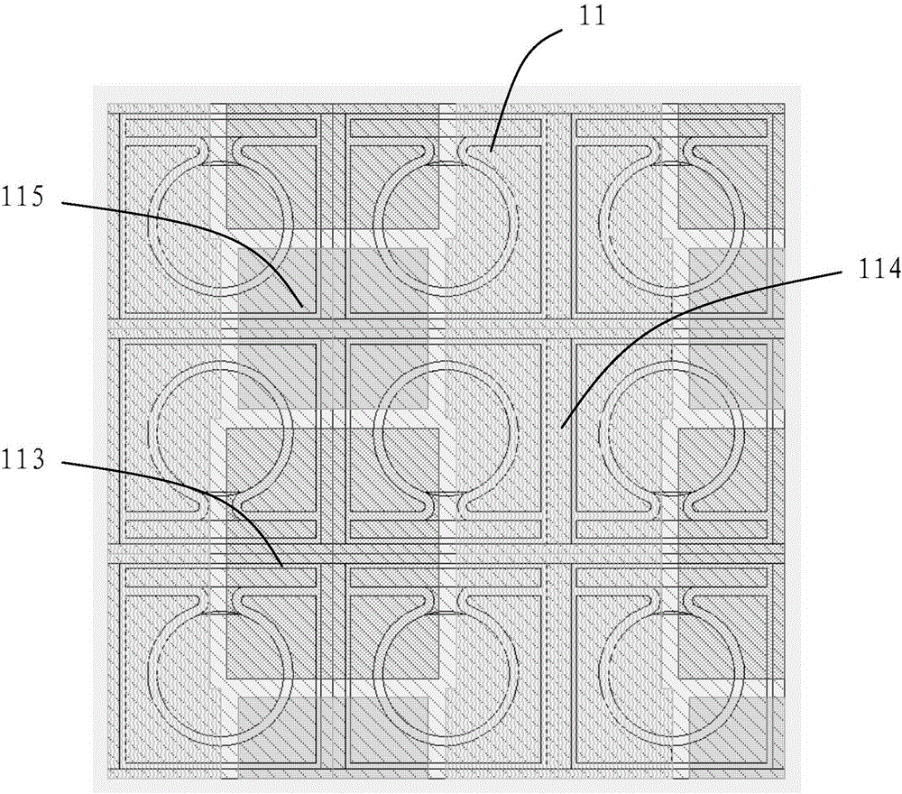
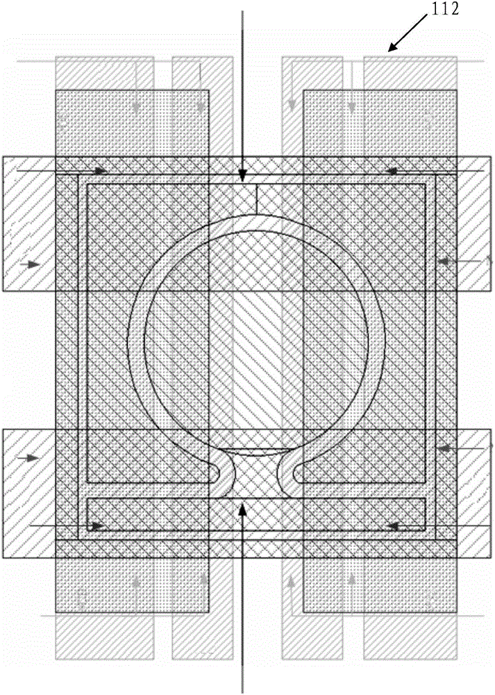
[0024] see first figure 1 and Figure 6 ,in, figure 1 It is a schematic structural diagram of the induction unit block circuit of the present invention, Figure 6 It is a schematic diagram of the overall structure of the sensing unit, the second and the third ESD protection unit of an ESD protection-based biometric sensing device of the present invention. A biometric sensing device based on ESD protection of the present invention includes a sensing unit 10 , a second ESD protection unit 20 and a third ESD protection unit 30 . In the present invention, the electrostatic current acting on the inducti...


PUM


Abstract

The invention discloses a biological recognition sensing device based on electronic static discharge (ESD) protection. The biological recognition sensing device comprises a sensing unit array. The sensing unit array comprises multiple sensing units which are arranged at intervals. By first ESD protection units which are arranged in the sensing units, ESD currents flow out of the sensing units. The first ESD protection units which are arranged in the sensing units accelerate the ESD currents to flow out of a working circuit, thus the ESD protection of the sensing units is achieved and ESD protection ability of the circuit is improved.

Description

technical field [0001] The invention relates to the technical field of touch screens, in particular to an ESD protection-based biometric identification sensing device. Background technique [0002] ESD protection has always been an important topic, especially after entering the deep submicron process, with the reduction of related dimensions, the ESD protection capabilities of various devices and circuits decline rapidly, so the design of ESD protection circuits is in a more prominent position Location. [0003] Currently, for general IC design, ESD protection is generally handled on pads (circuit pins). Because the entire chip except the pad is packaged with a plastic package, this effectively isolates the circuit inside the IC from the external space. But for biometric ICs, the entire sensing array is directly in contact with the external space, exposed to the outside, and also in direct contact with the organism to be identified (such as hands, clothes, etc.), at this t...

Claims


Application Information

Patent Timeline
Patent Type & Authority Patents(China)
IPC IPC(8): G06F3/041H01L27/02
Inventor 程泰毅赵祥桂
Owner SILEAD
Why Eureka
Try Eureka