Manufacturing method and manufacturing apparatus of organic device and organic device

A technology for organic devices and manufacturing methods, which can be used in semiconductor/solid-state device manufacturing, lighting devices, electric solid-state devices, etc., and can solve problems such as higher manufacturing costs and lower productivity.

Active Publication Date: 2014-09-17
TOKYO ELECTRON LTD
View PDF6 Cites 4 Cited by
  • Summary
  • Abstract
  • Description
  • Claims
  • Application Information

AI Technical Summary

Problems solved by technology

[0007] However, in Patent Document 1, a mask is required for film formation of the intermediate layer, and alignment between the mask and the substrate is required, so there is a problem that the productivity is lowered and the manufacturing cost is increased.

Method used


Image

  • Manufacturing method and manufacturing apparatus of organic device and organic device
  • Manufacturing method and manufacturing apparatus of organic device and organic device
  • Manufacturing method and manufacturing apparatus of organic device and organic device

Examples


Deformed example 1

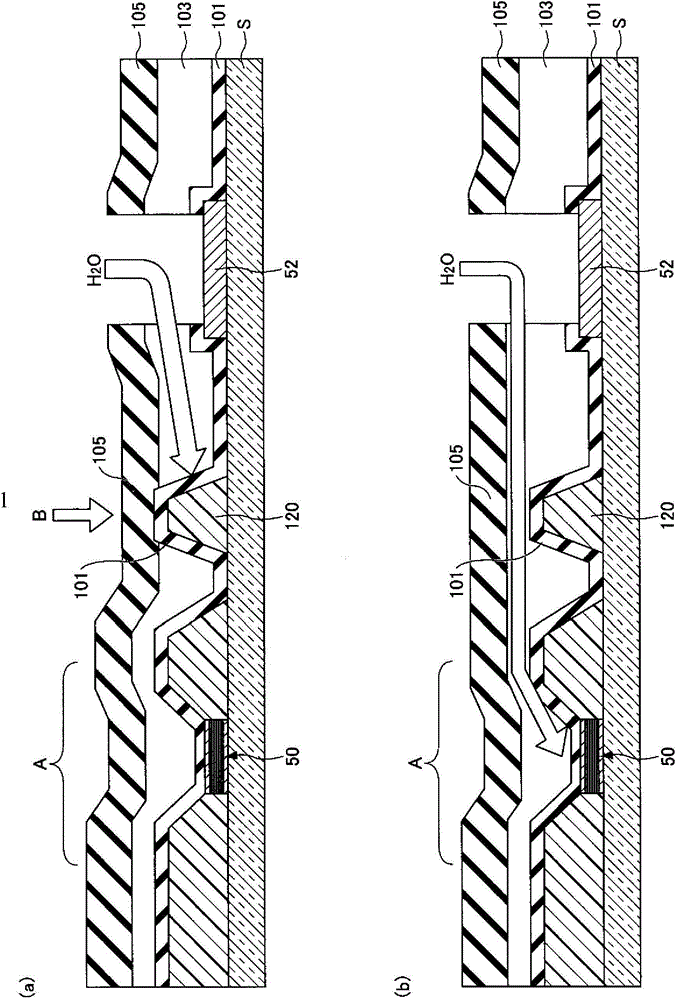
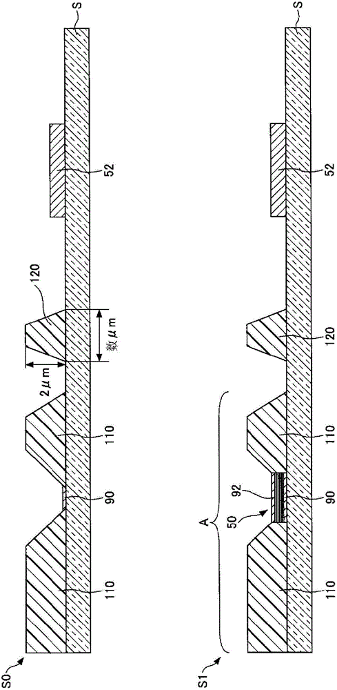
[0088] in Figure 3C In the case of "S5", at position B on the partition wall 120, the sealing layer 101 and the sealing layer 105 are brought into close contact with each other to form a wall, thereby blocking the penetration of moisture from the electrode pad 52 side. In contrast, in Modification 1, as Image 6 As shown in "S4", not only at position B on the partition wall 120, but also at positions C and D on the partition wall 110, the wall formed by the sealing layer 101 and the sealing layer 105 blocks moisture from Immersion on the electrode pad portion 52 side. At this time, such as Image 6 As shown in "S4", etch back is performed until the sealing layer 101 is exposed from the intermediate layer 103 at positions B, C, and D. Thus, as Image 6 As shown in "S5", the sealing layer 105 is in contact with the sealing layer 101 exposed from the intermediate layer 103 at positions B, C, and D.

[0089] With the above structure, the wall portions formed at the positions B, C, ...

Deformed example 2

[0091] In addition, in Modification 2, as Figure 7 As shown in "S4", not only at positions B, C, D on the partition wall portions 110 and 120, but also at positions E and F where the partition wall portion 110 is not formed, the sealing layer 101 and the sealing layer 105 also contact each other. In the manufacturing process, such as Figure 7 As shown in "S4", the etch back is performed until the sealing layer 101 is exposed from the intermediate layer 103 at positions B, C, D, E, and F. In this case, the intermediate layer 103 is formed only on the side surface of the partition wall. Thus, as Figure 7 As shown in "S5", the sealing layer 105 formed on the intermediate layer 103 is in contact with the sealing layer 101 exposed from the intermediate layer 103 at positions B, C, D, E, and F.

[0092] With the above structure, the wall portions formed at the positions B, C, D, E, and F can more reliably block moisture, and thus can more reliably suppress the intrusion of moisture ...

Deformed example 3

[0094] In Modification 3, the formation of the intermediate layer and the etch back are repeatedly performed. For example, a substrate having an intermediate layer 103 formed after the sealing layer 101 having a thickness of 100 nm to 500 nm is formed Figure 7 "S4" shows the etch back of the intermediate layer 103. After that, like Figure 8A As shown in "S4-1", the intermediate layer 103 is formed again. Next, like Figure 8A As shown in "S4-2", the formed intermediate layer 103 is etched back again. Next, like Figure 8B The sealing layer 105 is formed as shown in "S5-1". Here, the formation and etch-back of the intermediate layer 103 are repeatedly performed twice, but the number of repetitions of the formation and etch-back of the intermediate layer 103 is not limited to this.

[0095] Next, like Figure 8C As shown in "S6-1", the cover sheet 107 is attached with an adhesive (adhesive layer) so that the cover sheet 107 covers the organic EL element 50. Thereby, the mechan...


PUM


Abstract

The invention provides a manufacturing method and a manufacturing apparatus of an organic device and the organic device capable of inhibiting water from immersing into an organic EL element. The method comprises an input step and an etch-back step. In the input step, a substrate with an intermediate layer formed above a first sealing layer is inputted, and the first sealing layer is used for sealing an organic layer on an anode of one or multiple separating wall portions. In the etch-back step, the intermediate layer formed in the substrate is etched back until at least one part of the first sealing layer of at least one of the one or multiple separating wall portions is exposed from the intermediate layer and can contact with a second sealing layer formed in the next step.

Description

Technical field [0001] The invention relates to a manufacturing method of an organic device, a manufacturing apparatus of an organic device, and an organic device. Background technique [0002] In recent years, organic EL elements such as electroluminescence (EL: electro Luminescence) have been developed. The organic EL element has the following advantages: it consumes less power than a braun tube or the like, and it emits light by itself and has an excellent viewing angle compared to a liquid crystal display. [0003] On the other hand, organic EL elements are afraid of water. Therefore, when moisture penetrates from the defective part of the organic EL element, it may cause a decrease in light-emitting brightness or produce a non-light-emitting area called a dark spot. Therefore, it is sometimes necessary to form, for example, a sealing layer having moisture permeability resistance on the surface of the organic EL element. In this case, as a sealing layer that is formed by a l...

Claims


Application Information

Patent Timeline
Patent Type & Authority Applications(China)
IPC IPC(8): H01L51/56H01L51/52H05B33/04H05B33/10
CPCH05B33/04H05B33/10H10K50/841H10K50/844H10K71/00H10K59/122H10K50/84H10K50/8428
Inventor 石川拓林辉幸
Owner TOKYO ELECTRON LTD
Why Eureka
Try Eureka