

Semiconductor Structure Including A Transistor Having A Layer Of A Stress-creating Material, And Method For The Formation Thereof
A semiconductor and transistor technology, applied in the field of integrated circuits
- Summary
- Abstract
- Description
- Claims
- Application Information
AI Technical Summary
Problems solved by technology
Method used
Image

Examples
Embodiment Construction
[0035] While the present disclosure is described with reference to the illustrative embodiments shown in the following detailed description and drawings, it should be understood that the following detailed description and drawings are not intended to limit the present disclosure to the specific embodiments disclosed; The embodiments are intended merely to illustrate various aspects of the subject matter disclosed herein, the scope of which is defined by the appended claims.
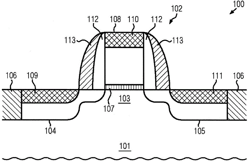
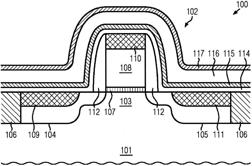
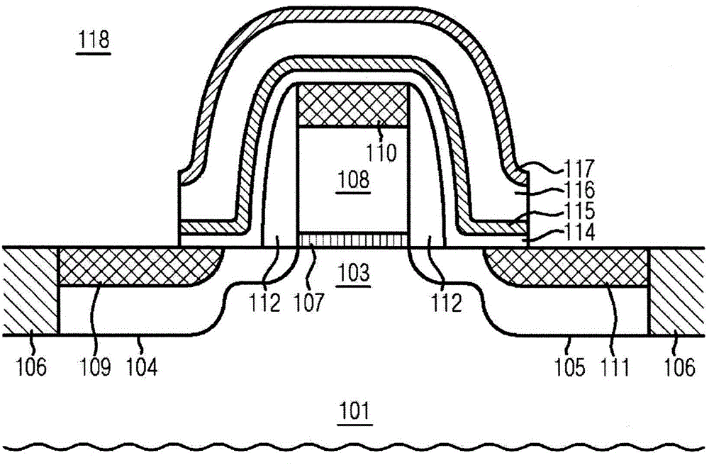
[0036] The present disclosure provides a transistor having disposed therein a layer of stress-creating material that provides a stress that varies in response to a signal applied to the layer of stress-creating material. The layer of stress-creating material may be arranged to provide stress at least in the channel region and, optionally, in the source and / or drain regions of the transistor. The stress provided by the layer of stress-creating material varies in response to a signal applied to the layer of...
PUM
 Abstract
Description
Claims
Application Information