Silicon-chip storage management method

A management method, silicon chip technology, applied to memory recording carrier reading problems, conveyor objects, electrical components, etc., can solve problems such as inability to perform chip transfer, inaccurate silicon chip information, accidents, etc., to avoid chip selection errors , to avoid imprecise effects

Inactive Publication Date: 2014-10-01
SHANGHAI HUALI MICROELECTRONICS CORP
View PDF4 Cites 0 Cited by
  • Summary
  • Abstract
  • Description
  • Claims
  • Application Information

AI Technical Summary

Problems solved by technology

[0004] However, if figure 1 As shown, there is no RFID on the wafer escape box 100, so the silicon wafer sorter cannot identify the information of the silicon wafers therein. Therefore, according to the prior art, the transfer of wafers in the wafer escape box can only be done offline. (Offline) film transfer (that is, need to manually select the silicon wafers to be transferred on the wafer sorter), and cannot perform online (Online) film transfer on the manufacturing execution system MES (manufacturing execution system) (that is, cannot execute automatic upload)
[0005] For the wafer escape box 100, manual selection of silicon wafers to be transported on the wafer sorter is likely to cause errors in wafer selection due to human negligence and thus cause accidents.
On the other hand, it is easy to cause inaccurate silicon wafer information due to human negligence

Method used


Image

  • Silicon-chip storage management method
  • Silicon-chip storage management method
  • Silicon-chip storage management method

Examples


Embodiment Construction

[0020] In order to make the content of the present invention clearer and easier to understand, the content of the present invention will be described in detail below in conjunction with specific embodiments and accompanying drawings.

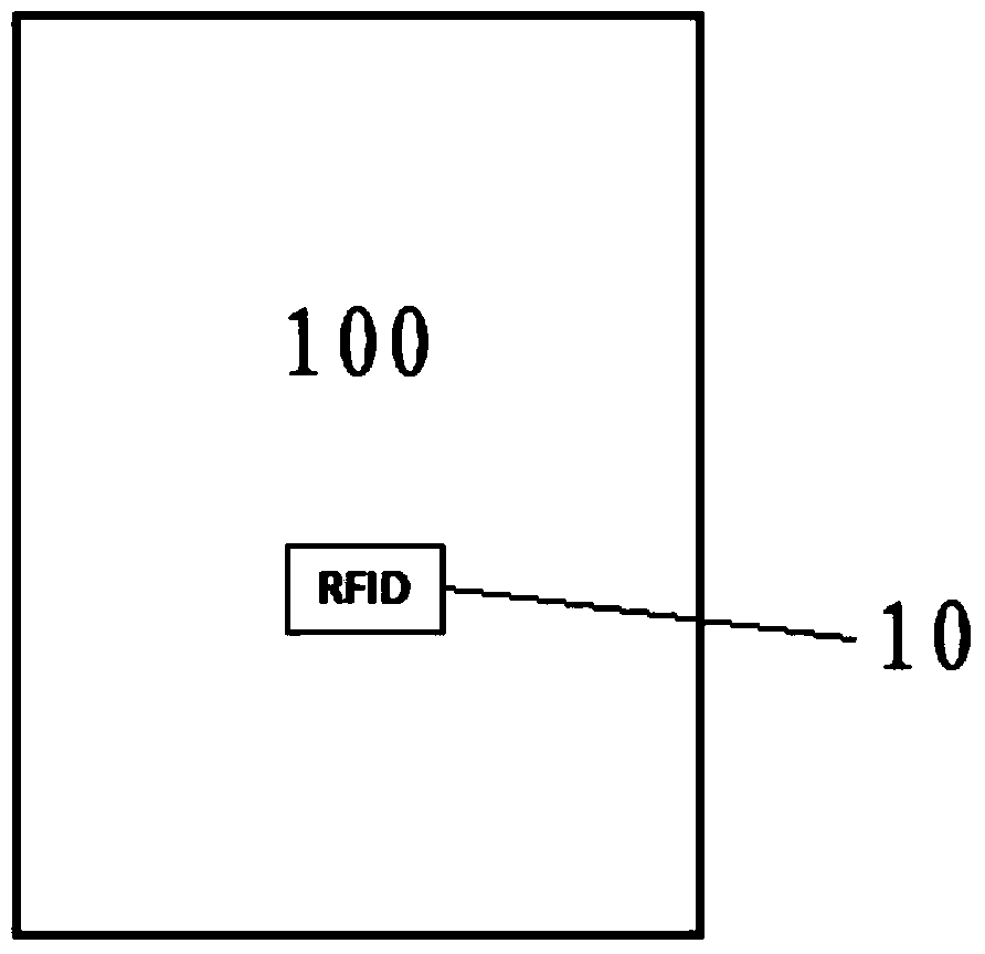
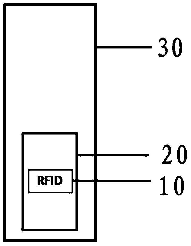
[0021] Regardless of the wafer transfer box FOUP (Front Opening Unified Pod) or the wafer transfer box FOSB (Front Opening Shipping Box), if you want to automatically upload wafers to the wafer sorter online, you need an RFID tag to perform online automatic wafer transfer; However, there is no RFID tag on the existing wafer escape box, so it cannot be automatically transferred online on the silicon wafer sorter. Thus, the present invention pastes the RFID label with the written virtual identification code (for example, virtual identification symbol) on the wafer escape box by refitting the RFID label, and then it can be successfully placed on the wafer sorter for online automatic transmission. piece.

[0022] Preferred embodiments of the presen...


PUM


Abstract

The invention provides a silicon-chip storage management method. The silicon-chip storage management method comprises the following steps that an RFID tag adheres to a white card, the white card is placed in a plastic bag, and the plastic bag adheres to the surface of a front opening shipping box; a virtual identification code is assigned to the RFID tag, so that each RFID tag corresponds to the unique virtual identification code; the front opening shipping box is placed at a first silicon-chip conveying port of a silicon-chip sorter, a silicon-chip front opening unified pod is placed at a second silicon-chip conveying port of the silicon-chip sorter, the silicon-chip sorter is used for obtaining the unique virtual identification code by reading the RFID tag, and therefore automatic conveying of silicon chips is conducted on the silicon-chip sorter. The silicon-chip storage management method can be used for achieving online conveying of the silicon chips in the front opening shipping box on a manufacturing execution system. According to the silicon-chip storage management method, the problem that human errors lead to wrong chip selection and therefore accidents are caused can be solved, and inaccurate silicon-chip information caused by the human errors can be avoided.

Description

technical field [0001] The invention relates to the field of semiconductor manufacturing, and more specifically, the invention relates to a storage management method for silicon wafers. Background technique [0002] Currently, front opening unified pods (FOUP) and front opening shipping boxes (FOSB) are generally used in the semiconductor industry as containers for carrying, transporting and protecting wafers. [0003] For the silicon wafers in the wafer transport box, the existing silicon wafer sorter (sorter) reads and confirms the silicon wafer information through the radio frequency identification RFID (Radio Frequency Identification) tag on the wafer transport box . [0004] However, if figure 1 As shown, there is no RFID on the wafer escape box 100, so the silicon wafer sorter cannot identify the information of the silicon wafers therein. Therefore, according to the prior art, the transfer of wafers in the wafer escape box can only be done offline. (Offline) film tr...

Claims


Application Information

Patent Timeline
IPC IPC(8): H01L21/67H01L21/677
CPCH01L21/6773G06K7/0008H01L21/67703
Inventor 郑小平
Owner SHANGHAI HUALI MICROELECTRONICS CORP
Why Eureka
Try Eureka