
Transparent conducting film and touch device

A technology of transparent conductive film and conductive unit, applied in the input/output of user/computer interaction, computer parts, graphic reading, etc., can solve the problems of multi-electrode leads, etc., to increase the area, improve the utilization rate, and reduce the number of Effect

Inactive Publication Date: 2014-10-15
NANCHANG O FILM TECH CO LTD +2
View PDF9 Cites 0 Cited by
  • Summary
  • Abstract
  • Description
  • Claims
  • Application Information

AI Technical Summary

Problems solved by technology

[0005] The present invention provides a transparent conductive film, which is used to solve the problem that the existing transparent conductive film has more electrode leads, and further provides a touch device comprising the transparent conductive film

Method used


Image

  • Transparent conducting film and touch device
  • Transparent conducting film and touch device
  • Transparent conducting film and touch device

Examples


Embodiment 2

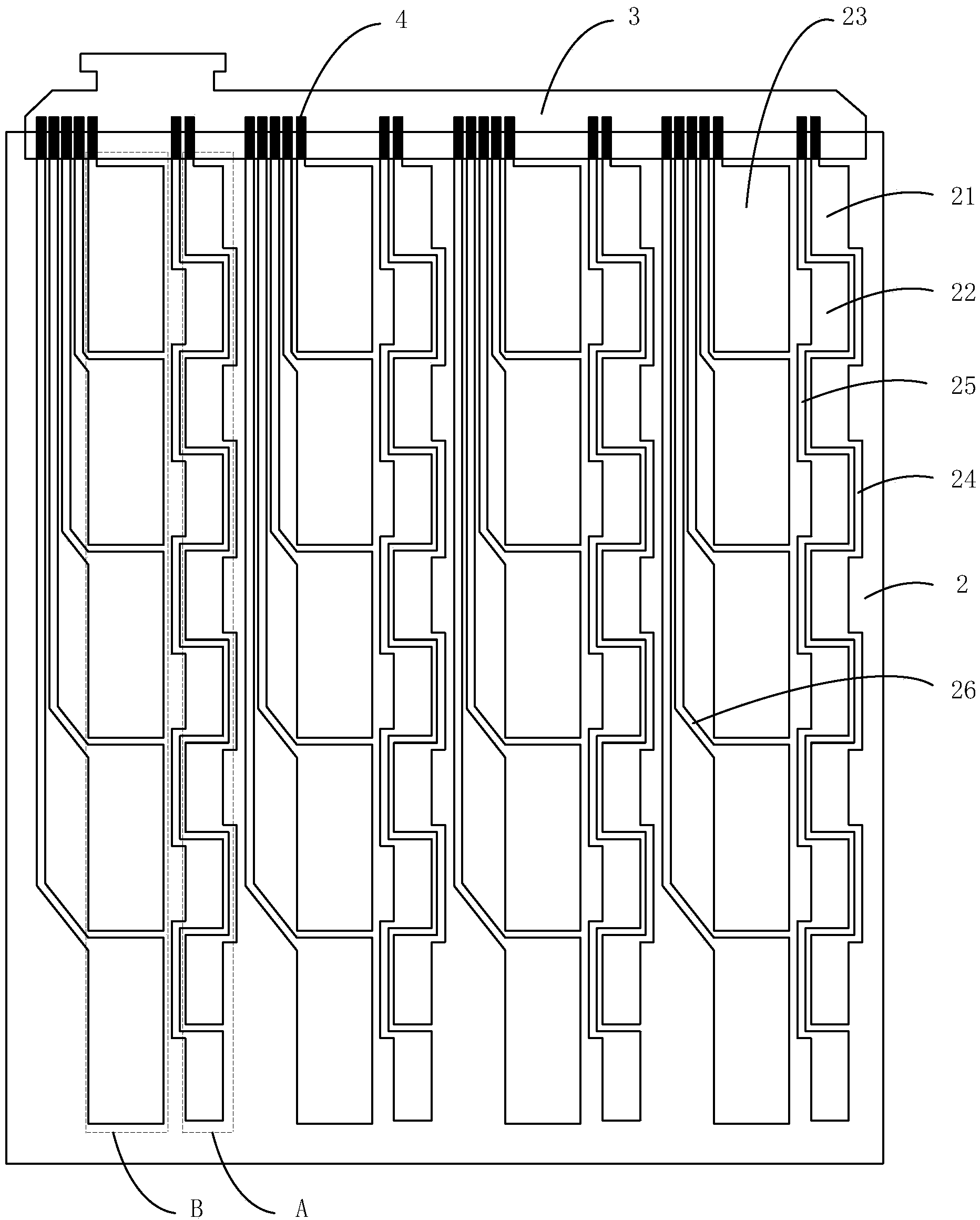
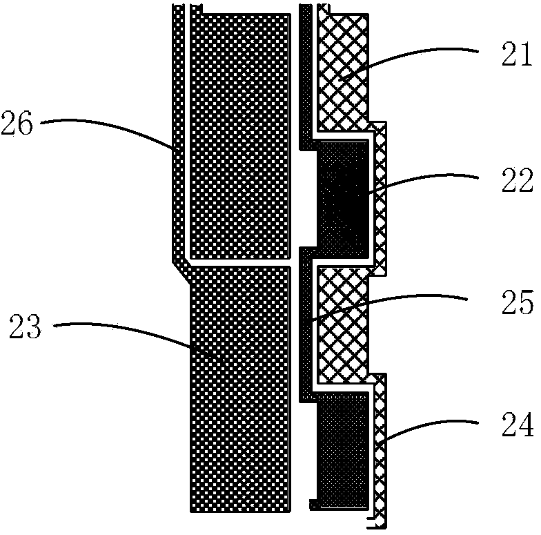
[0070] figure 2 The illustrated embodiment provides an implementation of a transparent conductive film, wherein the first conductive unit 21 and the second conductive unit 22 have the same shape and the same size, then when the first conductive unit 21 and the second conductive unit 22 When arranged in a row, the first connection lines 24 need to bypass the second conductive unit 22 to form a protrusion, and the second connection lines 25 also need to bypass the first conductive unit 21 to form a protrusion structure.

[0071] Figure 7 The schematic diagram of the structure of the transparent conductive film provided by Embodiment 2 of the present invention. This embodiment optimizes the structure of the transparent conductive film on the basis of the above embodiments, as shown in Figure 7 As shown, in this embodiment, the distances between the first conductive unit 21 and the second conductive unit 22 relative to the same third conductive unit 23 are different, wherein t...

Embodiment 3

[0074] Figure 8 A schematic structural diagram of a group of corresponding first conductive units, second conductive units and third conductive units in the transparent conductive film provided by Embodiment 3 of the present invention. This embodiment optimizes the structure of the transparent conductive film on the basis of the above embodiments, such as Figure 8 As shown, the first conductive unit 21, the second conductive unit 22 and the third conductive unit 23 are each provided with at least one branch, wherein the branch 211 of the first conductive unit 21 and the branch 231 of the third conductive unit 23 alternate along the column direction Arranged, the branches 221 of the second conductive unit 22 and the branches 231 of the third conductive unit 23 are also arranged alternately along the column direction.

[0075] Specifically, the first conductive unit 21 is provided with four first branches 211, the second conductive unit 22 is provided with four second branche...


PUM


Abstract

The invention provides a transparent conducting film and a touch device. The transparent conducting film comprises a transparent substrate, a first array of electrode and a second array of electrode, wherein the first array of electrode and the second array of electrode are arranged on the transparent substrate; the first array of electrode comprises first conducting units and second conducting units, wherein the first conducting units and the second conducting units are alternately arranged; the second array of electrode comprises third conducting units which are arranged at an interval; the first conducting units in the same array are connected in series; the second conducting units in the same array are connected in series; and one third conducting unit independently corresponds to one first conducting unit and one second conducting unit to form a first pair of induction nodes and a second pair of induction nodes. The transparent conducting film and the touch device provided by the invention can improve the use ratio of an effective induction area.

Description

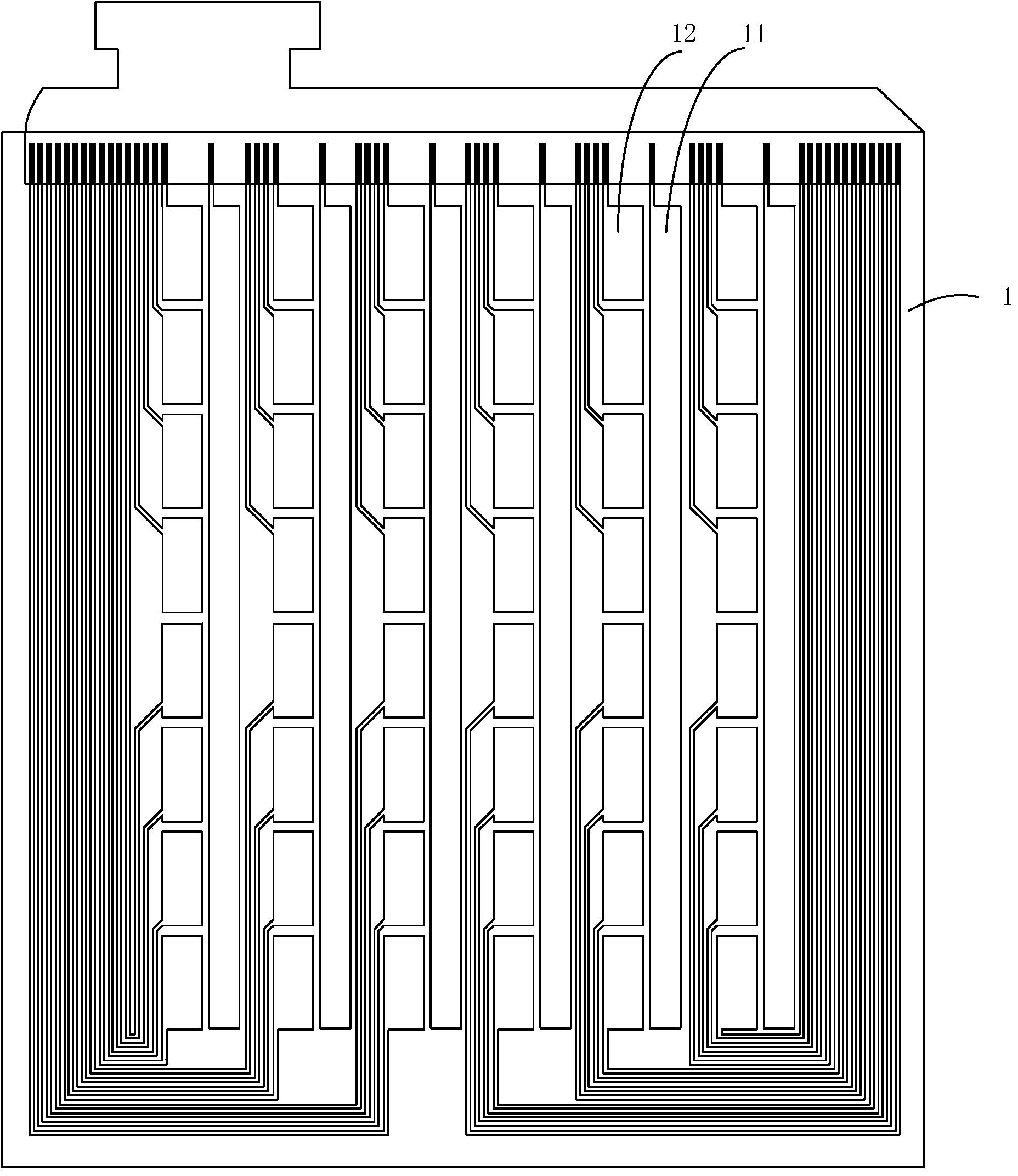
technical field [0001] The invention relates to electronic touch technology, in particular to a transparent conductive film and a touch device. Background technique [0002] As an inductive device that can receive input signals such as touch, the touch device has given a new look to information interaction and is a brand-new information interaction device. The transparent conductive film is an important part of the touch device, and is used to realize the function of obtaining the touch position and operating instructions. [0003] figure 1 It is a schematic diagram of the structure of the existing transparent conductive film, such as figure 1 As shown, the transparent conductive film includes a transparent substrate 1, and a plurality of strip-shaped conductive units 11 and a plurality of block-shaped conductive units 12 arranged on the transparent substrate 1, wherein one strip-shaped conductive unit 11 forms the first column electrode, 8 A block-shaped conductive unit ...

Claims


Application Information

Patent Timeline
Patent Type & Authority Applications(China)
IPC IPC(8): G06F3/01
Inventor 唐根初刘伟蒋芳
Owner NANCHANG O FILM TECH CO LTD
Learn More