
semiconductor components

A semiconductor and component technology, applied in the field of power module semiconductor components, can solve problems such as exposure

Active Publication Date: 2019-11-08
FAIRCHILD SEMICON CORP
View PDF10 Cites 0 Cited by
  • Summary
  • Abstract
  • Description
  • Claims
  • Application Information

AI Technical Summary

Problems solved by technology

A portion of the end device and perhaps a portion of the die pad may be exposed externally from the encapsulation material

Method used


Image

  • semiconductor components
  • semiconductor components
  • semiconductor components

Examples


Embodiment Construction

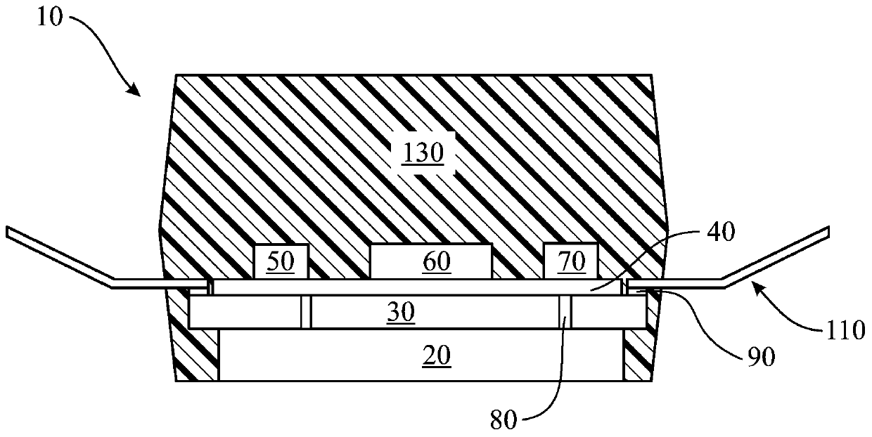
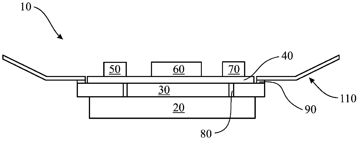
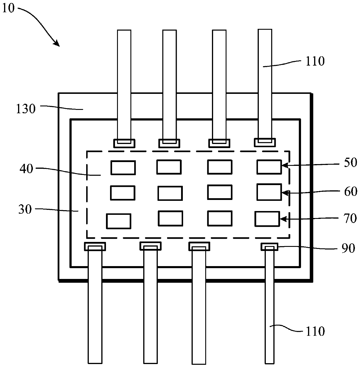
[0012] In order to provide a thorough understanding, the following description gives specific explanations. However, it will be understood by those skilled in the art that semiconductor devices and associated methods of using the devices may be practiced and used without application of these specific explanations. Indeed, the apparatus and associated methods may be practiced by modifying the illustrated apparatus and associated methods and may be used with any other apparatus and techniques customarily used in the industry. For example, while the following description focuses on methods that facilitate semiconductor components in the IC industry, it may be applicable or applied to other electronic devices such as automotive or white good modules, optoelectronic devices, solar cells, Memory structure, lighting control, power supply and amplifier, etc.

[0013] Some embodiments of power module semiconductor assemblies including flexible circuit boards and methods for manufactur...


PUM


Abstract

The invention discloses a semiconductor assembly, in particular a power module semiconductor assembly including a flexible circuit board and a method for manufacturing such an assembly. The semiconductor assembly includes a flexible circuit board, a conductive film on a first portion of the upper surface of the flexible circuit board, a solder pad on a second portion of the upper surface of the flexible circuit board, a heat sink on a portion of the bottom surface of the flexible circuit board , passive components, separate devices, or IC devices connected to a part of the conductive film, and the leads of the lead frame connected to the pads. These components can have component placement with high design flexibility and easy wiring design, reducing the time to design the components and reducing the cost of the components. Other embodiments are also described.

Description

technical field [0001] The present application relates generally to semiconductor components and methods of making such components. More specifically, the present application describes power module semiconductor assemblies including flexible circuit boards and methods of making such assemblies. Background technique [0002] Semiconductor components are known in the art. Typically, these components may include one or more semiconductor devices, such as integrated circuit (IC) chips, which may be connected to die pads that are collectively formed in a leadframe. Bond wires sometimes electrically connect the integrated circuit chip to a series of terminal devices that serve as power connections for external devices such as printed circuit boards ('PCBs'). Encapsulation materials may be used to cover bond wires, integrated circuit chips, terminal equipment, and / or other components to form the exterior of the semiconductor assembly. A portion of the end device and perhaps a po...

Claims


Application Information

Patent Timeline
Patent Type & Authority Patents(China)
IPC IPC(8): H01L23/498H01L25/16
CPCH01L2924/13055H01L2924/13091H01L2224/48091H01L2224/48247H01L2924/00014H01L2924/00
Inventor 杜安·A·休斯
Owner FAIRCHILD SEMICON CORP
Learn More