A combined waveguide
A technology of waveguide and waveguide port, which is applied in the field of communication to achieve the effect of improving insertion loss, reducing processing difficulty and cost, and improving loss
- Summary
- Abstract
- Description
- Claims
- Application Information
AI Technical Summary
Problems solved by technology
Method used
Image
Examples
Embodiment 1
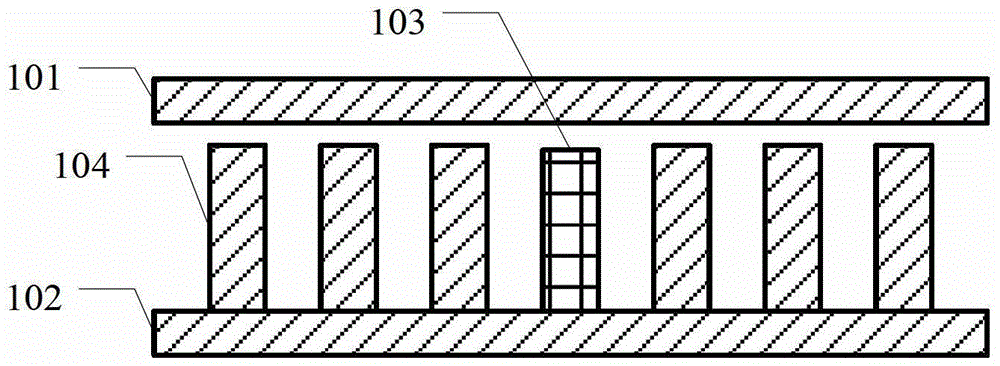
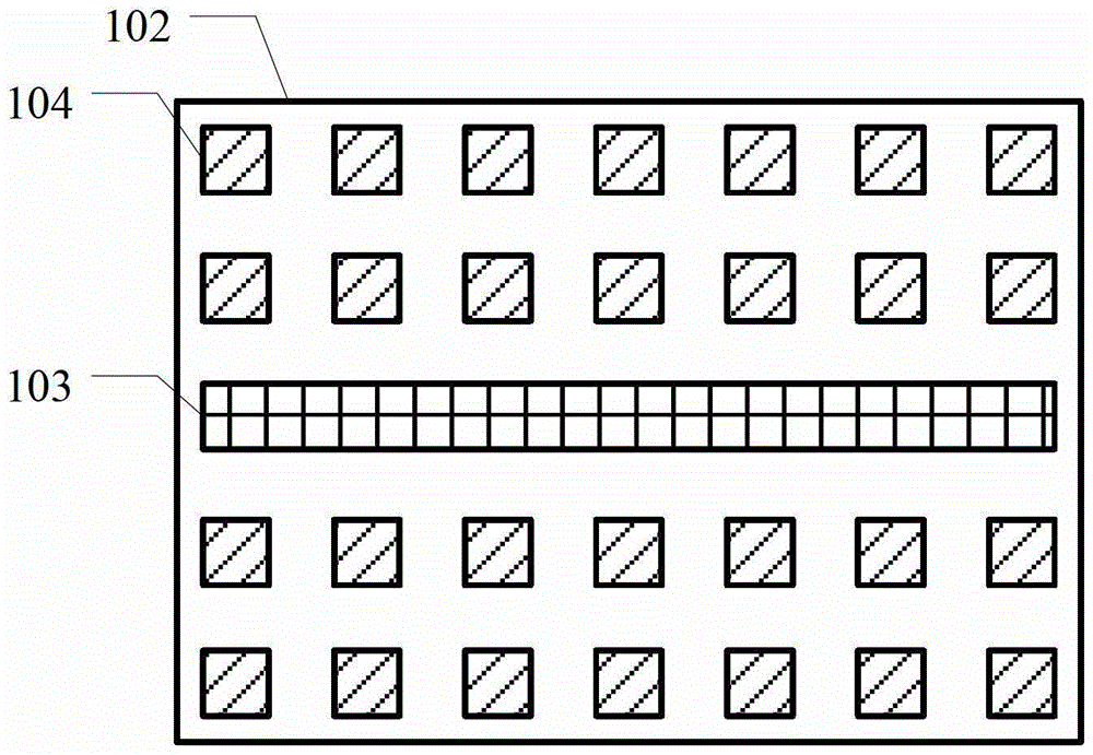
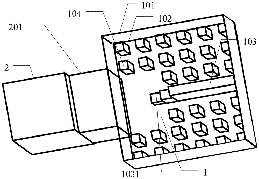
[0060] image 3 It is a three-dimensional schematic diagram of a horizontal transition structure between a gap waveguide and a rectangular waveguide according to an embodiment of the present invention, Figure 4 It is a schematic diagram of the right side view of the transition structure of the rectangular waveguide described in the embodiment of the present invention, Figure 5 It is a schematic front view of the horizontal transition structure between the gap waveguide and the rectangular waveguide according to the embodiment of the present invention, Image 6 It is a schematic top view of the horizontal transition structure between the gap waveguide and the rectangular waveguide according to the embodiment of the present invention, as shown in Figure 3 to Figure 6 As shown, in the combined waveguide described in Embodiment 1 of the present invention, the horizontal transfer structure of the gap waveguide and the rectangular waveguide specifically includes:
[0061] The r...
Embodiment 2
[0071] Figure 8 It is a three-dimensional schematic diagram of a vertical transition structure between a gap waveguide and a rectangular waveguide according to an embodiment of the present invention, Figure 9 It is a schematic diagram of the right side view of the vertical transition structure between the gap waveguide and the rectangular waveguide according to the embodiment of the present invention, Figure 10 It is a schematic top view of the vertical transition structure between the gap waveguide and the rectangular waveguide according to the embodiment of the present invention, as shown in Figure 8 to Figure 10 As shown, in the combined waveguide described in Embodiment 2 of the present invention, the vertical transfer structure of the gap waveguide and the rectangular waveguide specifically includes:
[0072] The upper plate 101 of the air gap waveguide has a rectangular opening 1011, one side of the rectangular opening 1011 is perpendicular to the ridge 103 of the a...
Embodiment 3
[0082] Figure 11 It is a three-dimensional schematic diagram of the horizontal transfer structure between the gap waveguide and the microstrip line according to the embodiment of the present invention, Figure 12 It is a schematic top view of the gap waveguide and the microstrip line horizontal transition structure according to the embodiment of the present invention, Figure 13 It is a schematic front view of the gap waveguide and the microstrip line horizontal transfer structure of the embodiment of the present invention, as shown in Figure 11 to Figure 13 As shown, in the combined waveguide described in Embodiment 3 of the present invention, the structure of the horizontal transfer between the gap waveguide and the microstrip line specifically includes:
[0083] The upper plate 101 of the air gap waveguide is connected to the floor 301 of the microstrip line or the upper plate 101 of the air gap waveguide and the floor 301 of the microstrip line are all arranged on the s...
PUM
 Abstract
Description
Claims
Application Information


