Large-area uniform raman detection chip for porous membrane sensitivity enhancing and preparation method for large-area uniform raman detection chip

A detection chip and porous film technology, applied in the field of optical detection, can solve the problems of complex SERS chip process, high cost, fingerprint Raman signal interference, etc. Effect

Active Publication Date: 2015-03-11
INST OF ELECTRONICS CHINESE ACAD OF SCI
View PDF8 Cites 7 Cited by
  • Summary
  • Abstract
  • Description
  • Claims
  • Application Information

AI Technical Summary

Problems solved by technology

[0006] In the process of realizing the present invention, the applicant found that the SERS chip with good repeatability and high sensitivity prepared by the prior art requires complex processes and high costs, and it is difficult to avoid the generation of electromagnetically enhanced metal nanostructures and molecules to be tested. Especially the interference of the Raman signal of the fingerprint of the molecule to be tested caused by the direct contact with the biomolecule to be tested

Method used


Image

  • Large-area uniform raman detection chip for porous membrane sensitivity enhancing and preparation method for large-area uniform raman detection chip
  • Large-area uniform raman detection chip for porous membrane sensitivity enhancing and preparation method for large-area uniform raman detection chip
  • Large-area uniform raman detection chip for porous membrane sensitivity enhancing and preparation method for large-area uniform raman detection chip

Examples


no. 1 example

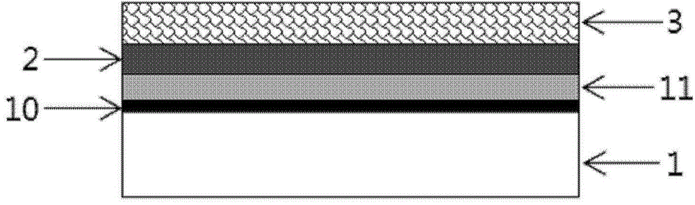
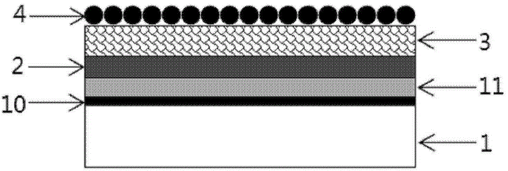
[0035] In the first exemplary embodiment of the present invention, a large-area uniform Raman detection chip sensitized by a porous membrane is proposed. Figure 1A It is a schematic cross-sectional view of a large-area uniform Raman detection chip sensitized by a porous membrane according to the first embodiment of the present invention. like Figure 1AAs shown, the large-area uniform Raman detection chip sensitized by the porous membrane comprises: a substrate 1; a transition film 10 formed on the upper surface of the substrate 1; a gold film 11 formed on the upper surface of the transition film 10; The reinforced structure film 2 is formed on the outer surface of the gold film 11, which is used as the electromagnetic enhancement layer of the Raman detection chip in this embodiment; the nanoporous film 3 is formed on the outer surface of the gold-based reinforced structure film 2 to enrich the To measure molecules, increase the number of molecules to be measured within the ra...

no. 3 example

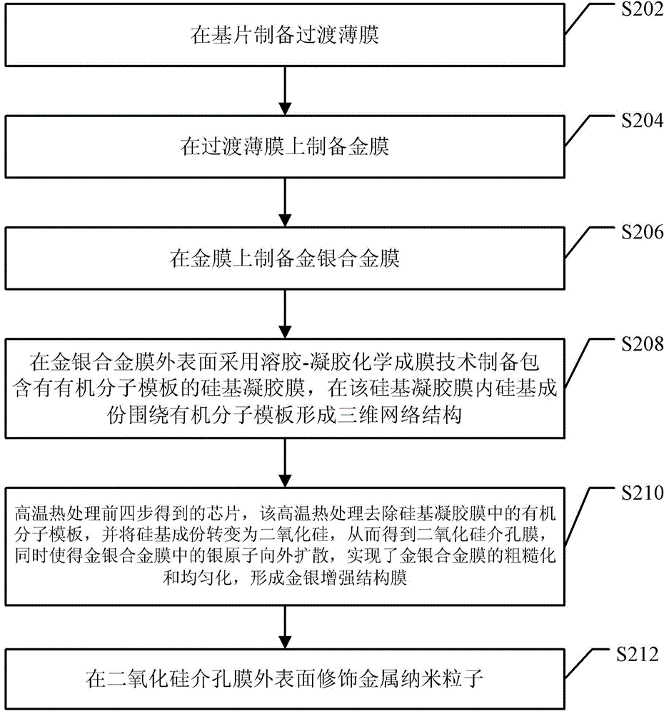
[0057] In the third exemplary embodiment of the present invention, a method for preparing the porous membrane-sensitized large-area uniform Raman detection chip described in the second embodiment is also provided. figure 2 It is a flowchart of a method for preparing a large-area uniform Raman detection chip sensitized by a porous membrane according to the third embodiment of the present invention.

[0058] Please refer to Figure 1 and figure 2 , the preparation method comprises:

[0059] Step S202: preparing a transition film 10 on the substrate 1;

[0060] Wherein, the substrate can be selected from one of flat glass, silicon wafer, ceramic wafer and metal wafer. Before preparing the transition film, the substrate needs to be cleaned. The cleaning process can be done according to the standard procedure.

[0061] The transition film is prepared by vacuum deposition technique on the upper surface of the cleaned substrate. The material of the transition film is chromium, ...


PUM

PropertyMeasurementUnit
thicknessaaaaaaaaaa
thicknessaaaaaaaaaa
pore sizeaaaaaaaaaa

Abstract

The invention provides a large-area uniform raman detection chip for porous membrane sensitivity enhancing and a preparation method for the large-area uniform raman detection chip. The raman detection chip comprises a substrate, a gold-based enhanced structural membrane which is formed on the substrate and is used as an electromagnetic enhancement layer of the raman detection chip, and a nano porous membrane which is formed on the outer surface of the gold-based enhanced structural membrane so as to enrich molecules to be detected. According to the large-area uniform raman detection chip for porous membrane sensitivity enhancing, the nano porous membrane serving as a molecule enriching layer can obviously increase the quantity of the molecules to be detected within a local enhanced electric field working range, so that the raman detection sensitivity of the chip is improved; the large-area uniform raman detection chip is particularly suitable for detection on small-molecular substances with ultralow concentration. The raman detection chip disclosed by the invention has the advantages of low preparation cost, high large-area uniformity and the like, and can suppress interference on a raman fingerprint diagram of the molecules to be detected due to metals.

Description

technical field [0001] The invention relates to the technical field of optical detection, in particular to a porous film sensitized large-area uniform Raman detection chip and a preparation method thereof. Background technique [0002] Raman scattering is a type of inelastic scattering. Due to the partial energy transfer between the incident light and the molecular vibration mode, the frequency of the scattered light changes compared with the incident light. This frequency shift is called Raman shift, which is closely related to the molecular structure. By measuring the Raman shift, it can be deduced Show molecular structure. [0003] Raman spectroscopy measurement methods are widely used in environmental monitoring, food safety testing, judicial identification, material analysis, biological science research and other fields. However, the Raman scattering cross section of most molecules is very small, making the Raman scattering light very weak, especially when the concent...

Claims


Application Information

Patent Timeline
Patent Type & Authority Applications(China)
IPC IPC(8): G01N21/65
Inventor 逯丹凤刘德龙祁志美
Owner INST OF ELECTRONICS CHINESE ACAD OF SCI
Why Eureka
Try Eureka