Method for detecting deafness genes based on surface enhanced Raman spectroscopy

A technology of surface-enhanced Raman and spectral detection, applied in the detection of deafness genes, based on surface-enhanced Raman spectroscopy in the field of detection of deafness genes, to achieve the effect of easy popularization and dissemination, overcoming poor reproducibility and good reproducibility

Inactive Publication Date: 2014-12-17
SUZHOU UNIV
View PDF6 Cites 10 Cited by
  • Summary
  • Abstract
  • Description
  • Claims
  • Application Information

AI Technical Summary

Problems solved by technology

[0005] At present, in the prior art, there is no detailed report on the highly sensitive and specific detection of deafness mutation genes in actual systems using surface-enhanced Raman spectroscopy

Method used


Image

  • Method for detecting deafness genes based on surface enhanced Raman spectroscopy
  • Method for detecting deafness genes based on surface enhanced Raman spectroscopy
  • Method for detecting deafness genes based on surface enhanced Raman spectroscopy

Examples


Embodiment 1

[0036] (1) Pretreatment process of silicon wafer

[0037] Take 1cm 2 3~6 large and small single silicon wafers are placed in a clean beaker and ultrasonicated with deionized water, acetone, and deionized water for 15 minutes in sequence to obtain silicon wafers with no impurities and organic substances on the surface for later use. Take 40mL of a mixed solution of 98wt% sulfuric acid and 30wt% hydrogen peroxide in a volume ratio of 3:1, and shake slowly while adding. Then put the silicon wafer into it and soak for 30 minutes to remove insoluble impurities, and then wash with deionized water for 3 to 5 times to remove the reaction solution for later use.

[0038] Soak the silicon wafer with 10wt% hydrofluoric acid for 20 minutes to remove the silicon dioxide oxide layer on the surface of the silicon wafer to form Si-H bonds on the surface of the silicon wafer. Quickly add 15mL of silver nitrate solution (2.5mM) with different pH values ​​and react for 20 minutes. According to...

Embodiment 2

[0044] (1) Pretreatment process of silicon wafer

[0045] Take 1cm 2 3~6 large and small single silicon wafers are placed in a clean beaker and ultrasonicated with deionized water, acetone, and deionized water for 15 minutes in sequence to obtain silicon wafers with no impurities and organic substances on the surface for later use. Take 40mL of a mixed solution of 98wt% sulfuric acid and 30wt% hydrogen peroxide in a volume ratio of 3:1, and shake slowly while adding. Then put the silicon wafer into it and soak for 30 minutes to remove insoluble impurities, and then wash with deionized water for 3 to 5 times to remove the reaction solution for later use.

[0046] Soak the silicon wafer with 15wt% hydrofluoric acid for 15 minutes to remove the silicon dioxide oxide layer on the surface of the silicon wafer to form Si-H bonds on the surface of the silicon wafer. Quickly add 20mL of silver nitrate solution (3mM) with different pH values ​​and react for 18 minutes. According to t...

Embodiment 3

[0052] (1) Pretreatment process of silicon wafer

[0053] Take 1cm 2 3~6 large and small single silicon wafers are placed in a clean beaker and ultrasonicated with deionized water, acetone, and deionized water for 15 minutes in sequence to obtain silicon wafers with no impurities and organic substances on the surface for later use. Take 40mL of a mixed solution of 98wt% sulfuric acid and 30wt% hydrogen peroxide in a volume ratio of 3:1, and shake slowly while adding. Then put the silicon wafer into it and soak for 30 minutes to remove insoluble impurities, and then wash with deionized water for 3 to 5 times to remove the reaction solution for later use.

[0054] Soak the silicon wafer with 10wt% hydrofluoric acid for 25 minutes to remove the silicon dioxide oxide layer on the surface of the silicon wafer, so that the Si-H bond is formed on the surface of the silicon wafer, and then spread the silicon wafer in a petri dish, with the shiny side facing up, facing it Quickly add...


PUM


Abstract

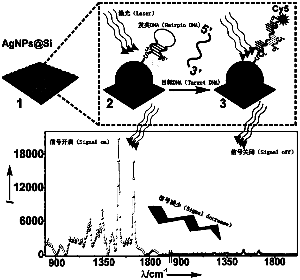
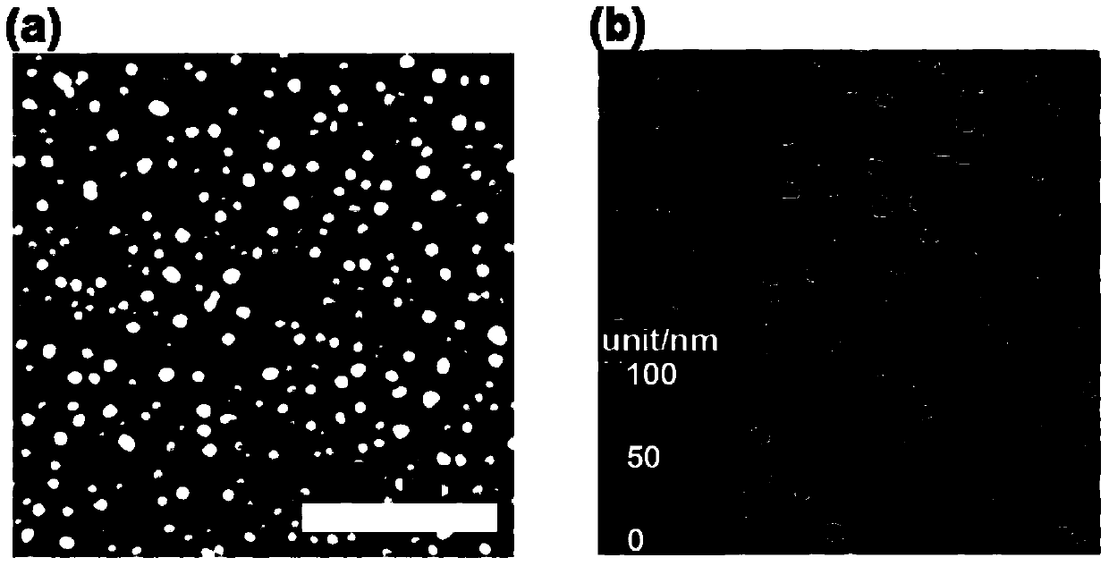
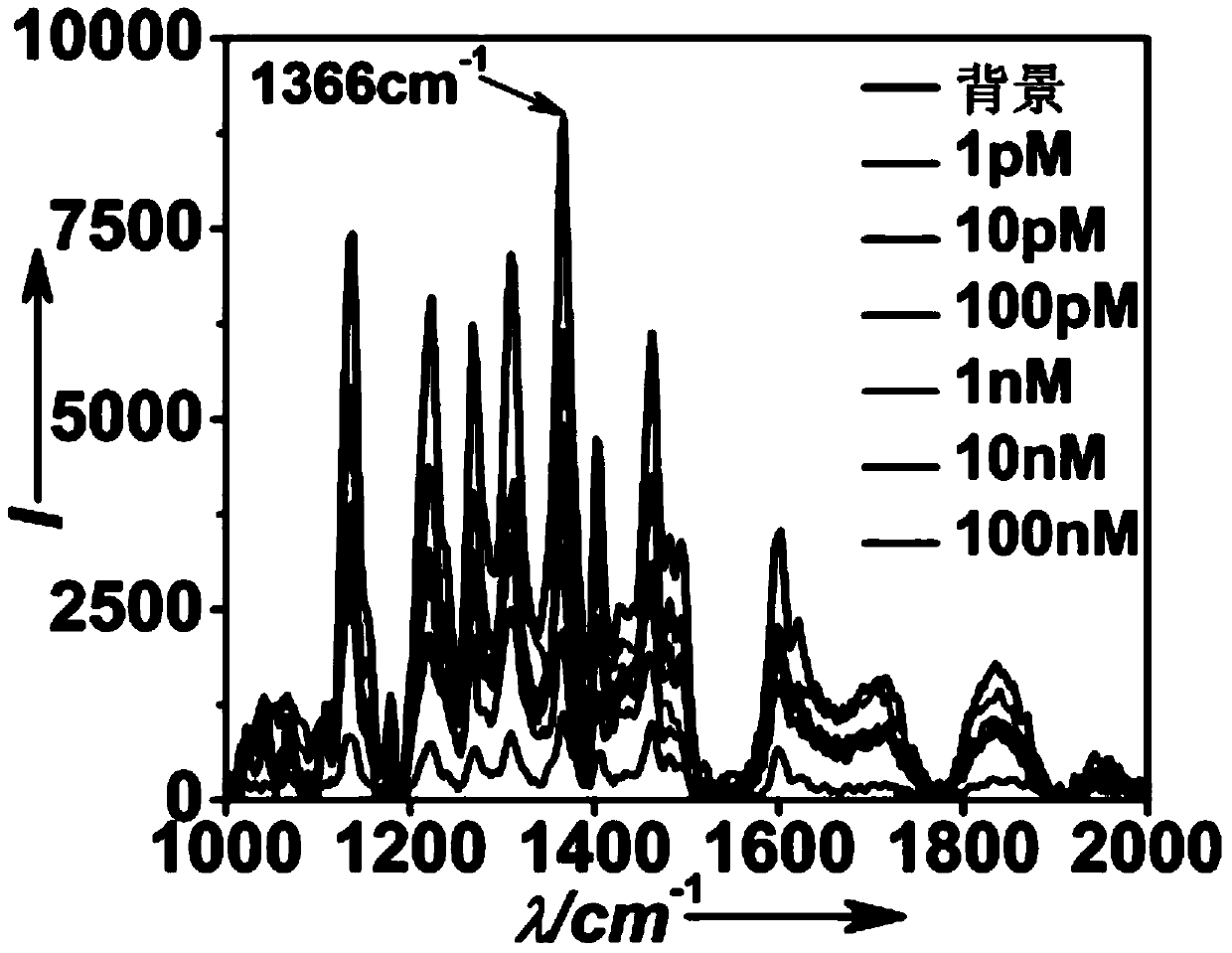
The invention discloses a method for detecting deafness genes based on the surface enhanced Raman spectroscopy. The method includes immersing a single crystal silicon wafer subjected to decontamination into hydrofluoric acid, forming a silicon-hydrogen bond on the surface of the wafer, adding nitric acid to acquire a silicon surface enhanced Raman scattering substrate, conducting covalence on hairpin DNA tail end sulfydryl and silver nanoparticles to form an Ag-S bond to enable the hairpin DNA to be in covalent connection onto a silicon wafer modified by the silver nanoparticles, after aging, adding the deafness causing gene sequence to be detected to conduct complete hybridization to conduct the surface enhanced Raman scattering (SERS) detection. According to the method, the SERS silicon substrate assited by the hairpin DNA to conduct detection of the deafness causing genes in the entity, the Raman detection sensitivity is effectively improved, the detection line is reduced, and the method has high specificity and good reproducibility, and is simple in operation, low in cost and easy to popularize and spread.

Description

technical field [0001] The invention belongs to the technical field of biological in vitro diagnosis and relates to a method for detecting deafness genes, in particular to a method for detecting deafness genes based on surface-enhanced Raman spectroscopy. Background technique [0002] Deafness is one of the most common human sensory system defects. Due to its complex etiology, high incidence and difficult treatment, it has long plagued patients and their surrounding groups, greatly affecting people's mutual communication and quality of life. According to statistics, the incidence of severe deafness in newborns is as high as 1 / 800~1 / 1000 (see: N.Engl.J.Med.2006, 354, 2151-2164), and almost 70 million people around the world suffer from 55 decibels or more More than 60% of people over the age of 70 have hearing loss of at least 25 decibels (see: Curr. Opin. Pediatr. 2012, 24, 679-686). [0003] The medical and scientific research circles have been working hard to find new tre...

Claims


Application Information

Patent Timeline
Patent Type & Authority Applications(China)
IPC IPC(8): G01N21/65
Inventor 何耀姜享旭王会
Owner SUZHOU UNIV
Why Eureka
Try Eureka