Polishing pad and method of making same

a technology of polishing pads and metallization layers, applied in the field of polishing pads, can solve the problems of excessive diffusion barrier and metallization materials, process performance drift, and inability to manufacture further metallization layers, and achieve the effect of superior uniformity and planarity

Inactive Publication Date: 2006-01-17
RIMPAD TECH
View PDF13 Cites 55 Cited by
  • Summary
  • Abstract
  • Description
  • Claims
  • Application Information

AI Technical Summary

Benefits of technology

[0026]In still another exemplary embodiment of the invention, the polymeric resin and gas mixture is forced through a high shear cavitation device which functions as yet another shearing application that causes the material to vaporize. High pressure drops are created which induces shearing. The high shear cavitation device may replace any of the other shearing applications, namely, sparging, the fine porosity stone mixer, the emulsifier, the homogenizing mixer, and any others, but may also be used in addition to these shearing applications to further control the size and uniformity of the cells contained within the resulting polishing pad. The high shear cavitation device does not require the separate use of a gas but may be used with the separate introduction of gas.
[0029]In accordance with another aspect of the invention, a surfactant and / or an ultraviolet stabilizer may be added to control the surface tension of the pad and / or control the shelf life of the pad, respectively.
[0030]In still another exemplary embodiment of the invention, a polishing pad having uniform microcellular size is produced by introducing a gas into a polymeric resin through a recirculating pump which pumps the polymeric resin and gas mixture through a fine porosity stone mixer, mixing the polymeric resin and gas mixture with an isocyanate to form a resulting mixture, and injecting the resulting mixture into a mold. In yet another exemplary embodiment of the invention, the polymeric resin and gas mixture may be passed through an emulsifier and / or a homogenizing mixer after being pumped through the fine stone porosity mixer to further control the uniformity and microcellular size of the pad.
[0031]As in the previously described exemplary embodiment, the polymeric resin and gas mixture may be forced through a high shear cavitation device which functions as yet another shearing application that causes the material to vaporize. High pressure drops are created which induces shearing. As previously stated, the high shear cavitation device may replace any of the other shearing applications, namely, sparging, the fine porosity stone mixer, the emulsifier, the homogenizing mixer, and any others, but may also be used in addition to these shearing applications to further control the size and uniformity of the cells contained within the resulting polishing pad. The high shear cavitation device does not require the use of a gas but may be used with the introduction of a gas.
[0032]In accordance with a further aspect of the invention, a method for making a polishing pad of uniform microcellular size is provided where the average cell size of the polishing pad is controlled by applying a plurality of shearing forces to the polymeric resin and gas mixture described above, prior to adding the isocyanate component. In accordance with a still further aspect of the invention, a window may be formed within the polishing pad to assist in end point detection. The window may be formed by removing a portion of the polishing pad and filling the opening created by the removed portion with either a liquid polymer material that solidifies as a transparent or translucent portion, or a solid transparent or translucent portion that is bonded to the pad. In addition, any other means known in the art for forming a window within a polishing pad may be used in accordance with the present invention.

Problems solved by technology

Without planarization, fabrication of further metallization layers becomes substantially more difficult due to the variations in the surface topography.
As a result of the pad and slurry consumables used and the process parameters employed in CMP processes, a phenomenon known as ‘glazing’ occurs in which the process performance drifts as a result of an inherent instability of the process.
Some excessive diffusion barrier and metallization material is also inevitably deposited over the field areas.
Manufacturability with respect to the pad amounts to the cost of the pad as a consumable, which is related to pad stability via pad life, as well as process capability in terms of process line yield limitations due to associated pad contribution to process capability.
A dominant issue within such art is the ability to control cell size.
The drawback of such processing stems from the violent exothermic reaction and the limited control over this process.
The Toray process cures the polyurethane under pressure at room temperature in an attempt to control cell size, but the resulting cell size is still large.
The Poval process uses a very large closed container system, which is again cured from the inside out, with large cell size and wide size distribution resulting from the poorly controlled reaction release of CO2.
Concentrations of nucleating agents greater than five parts per hundred parts polymer by weight leads to agglomeration, or insufficient dispersion of nucleating substance so that the diameter of the cell size becomes greater.
This gas is susceptible to coming out of solution as a result of a pressure drop.
A number of issues feed into pad stability and include the chemical integrity of the material as a result of its direct exposure to the polishing liquid (moisture absorption, chemical reactions), pad material curing at room temperature, mechanical property issues such as elasticity, plasticity, anelasticity and associated glazing response.
The distribution is generally accomplished by a combination of the movement of the preparation surface, the movement of the semiconductor wafer and the friction created between the semiconductor wafer and the preparation surface.” However, the importance of controlling friction and surface friction to maintain integrity of the target films, particularly those comprising low k dielectrics which may be porous and extremely fragile, is not addressed.
Research investigating the roll of the coefficient of friction (COF) has been performed and published by others, but they do not specifically target low COF processing, nor do they explicitly link such work to targeting low COF pad materials surfaces nor do they propose either micropores or the combination of low COF with micropores to achieve low friction during processing to avoid interfilm and intrafilm failure issues which occur during the polishing process, particularly in the regime of low k dielectrics.
They also immediately provide local slurry supply and thus limit frictional effects and ameliorate excursive contact effects which can result in intrafilm and interfilm failures.
The spacing and size of these artifacts are typically very regular and repetitive but more complex fractal patterns have been proposed.
Additionally, cell size creation though microelements or microspheres which dissolves in aqueous environments, leaves a polish pad and process susceptible to pad by-product induced defectivity.

Method used


Image

  • Polishing pad and method of making same
  • Polishing pad and method of making same
  • Polishing pad and method of making same

Examples


example 1

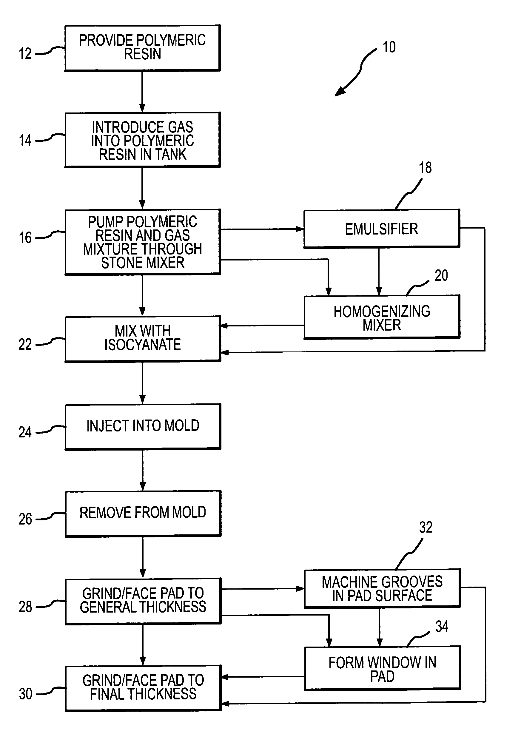
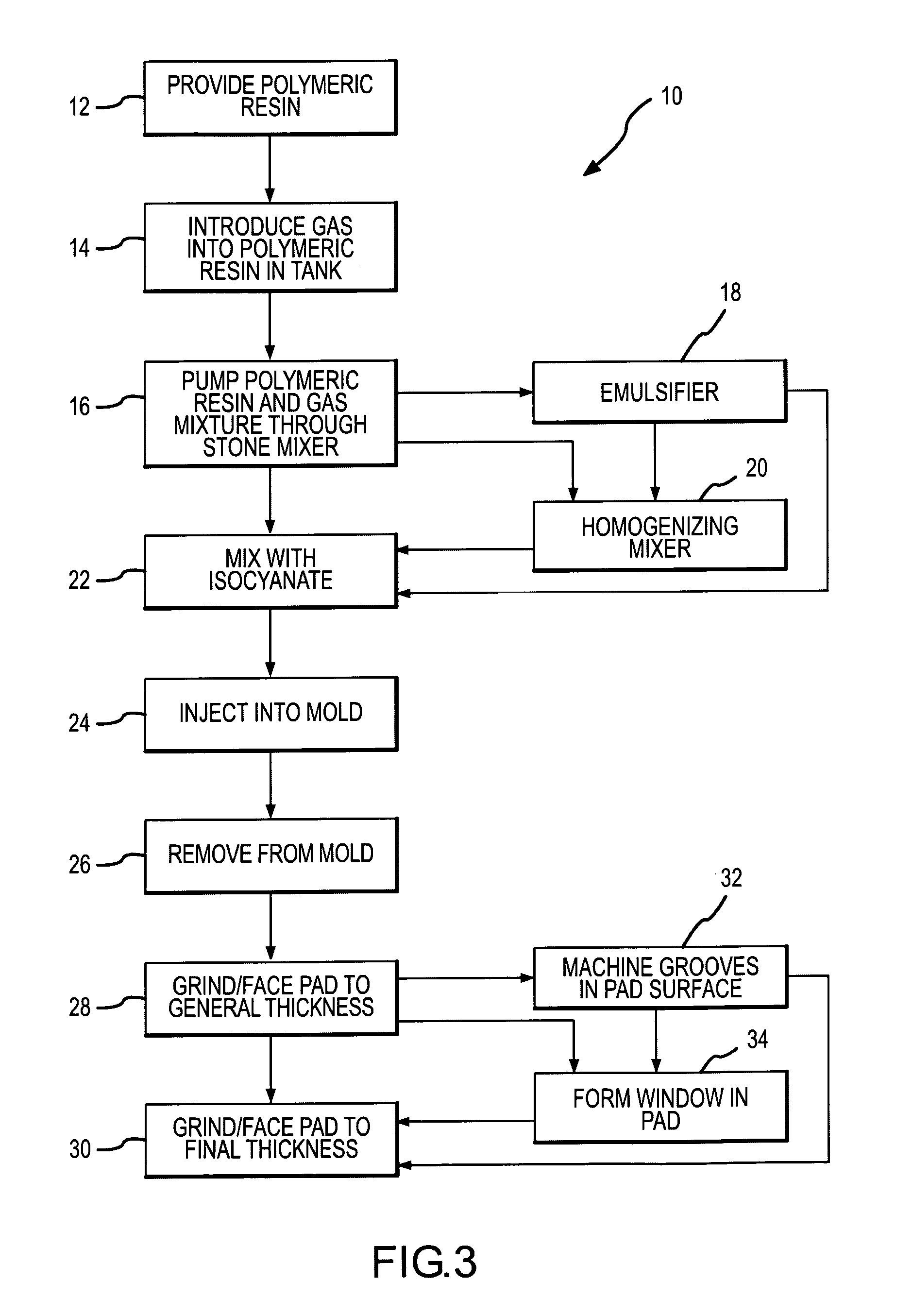
[0068]The apparatus as described in the attached FIGS. 3 and 4 was used in conjunction with an unaltered elastomeric polyurethane system supplied by Bayer, namely Bayflex XGT-140 which comprises a two component system. The equipment used was a 500 pound / min cylinder machine. The standard urethane supplier recommended process parameters were utilized for this example and include:

[0069]

Material Temperature 90–100 F.Mold Temperature140–158 F.Polyol Nucleation0.75–0.80Maximum Shot Time11–12 secTypical Demold Time 2–3 minIso / Polyol Volume Mixing Ration137:100

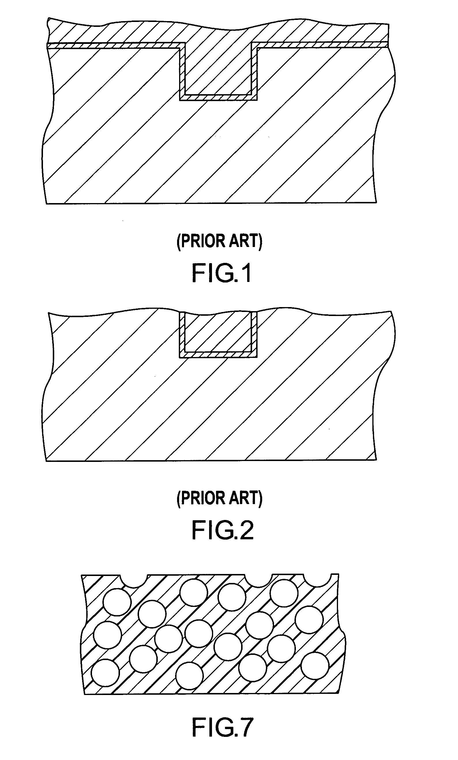
[0070]A closed cellular structured Polishing Pad was fabricated with the techniques and process guidelines as described. The average cell size for the polishing pad was 20 micrometers. Concentric grooves, 30 mil in depth, 62.5 mil wide with a radial density of eight grooves per inch were machined into the polishing surface. The pad was laminated with 3M 442KW double side adhesive and installed on a commercially available IPEC 472 pol...


PUM

PropertyMeasurementUnit
diameteraaaaaaaaaa
diameteraaaaaaaaaa
particle sizeaaaaaaaaaa

Abstract

An article or polishing pad for altering a surface of a work piece includes a polymer matrix created by reaction injection molding of size controlled gas bubbles within a polyurethane matrix. The proposed liquid urethane precursor is first injected into an actuated mold and cured. The molded product is then removed from the mold and double side faced or ground to form a single thin polishing pad comprising a single layer of homogeneous material.

Description

FIELD OF INVENTION[0001]The present invention generally relates to polishing pads used for creating a smooth, planar surface on a wide range of items such as glass, semiconductors, plastics and polymers, metals, dielectrics, and magnetic materials. More particularly, the present invention relates to the bulk structure of those pads and methods of making and using the same. The present invention also relates to an article of manufacture that is especially useful for polishing or planarizing a surface such as those used in manufacturing integrated circuits and MEM devices. In addition, the present invention is especially useful for polishing or planarizing metals and dielectrics such as those used in interconnect structures in integrated circuit devices such as semiconductor wafers containing copper damascene and dual damascene features.BACKGROUND OF THE INVENTION[0002]In the fabrication of optics, magnetic disks, micromachines, and particularly semiconductor integrated circuit device...

Claims


Application Information

Patent Timeline
Patent Type & Authority Patents(United States)
IPC IPC(8): B24D11/00B24B37/04B24D3/32B24D18/00B29C44/00B29C44/34
CPCB24B37/24B24D3/32B29C44/3442B24D18/00B24D18/0009B24D13/147B24D3/00B24D3/28H01L21/304
Inventor PRESTON, SPENCERHUTCHINS, DOUGHYMES, STEVE
Owner RIMPAD TECH
Why Eureka
Try Eureka