Light emitting diode device and manufacturing method thereof

a technology of light-emitting diodes and manufacturing methods, which is applied in the direction of discharge tubes/lamp details, discharge tubes luminescnet screens, plasma techniques, etc., can solve the problems of nanoscale quantum dots having different sizes, uniform distribution in the solution, and reducing the luminous efficiency of white led devices, so as to enhance the efficiency of leds and reduce light scattering effect. , the effect of raising the uniformity of nanocrystals

Active Publication Date: 2010-04-01
LITE ON ELECTRONICS (GUANGZHOU) LTD +1
View PDF2 Cites 25 Cited by
  • Summary
  • Abstract
  • Description
  • Claims
  • Application Information

AI Technical Summary

Benefits of technology

[0006]It is therefore a primary objective of the present invention to provide an LED device and a manufacturing method thereof so as to efficiently reduce light scattering effect to enhance the efficiency of LEDs using nanocrystal and raise uniformity of the nanocrystals.
[0007]The present invention forms the porous material layer with regular arrangement on the LED, and disposes the pores of the porous material layer with the nanocrystals so as to control the uniformity of the nanocrystals distributed in the phosphor layer. Therefore, the white light or the light of other colors formed by mixing the light emission from the LED and the nanocrystals can be uniform. With this technology, even to fabricate the white light emitting device with several chips or a chip array, the color quality can be believed to be very well.

Problems solved by technology

However, particles sizes of the phosphor material is several micrometers, incident visible light may be shielded and scattered by phosphor powders and the luminous efficiency of the white LED device will be reduced.
In the other hands, the nanoscale quantum dots will have different sizes and distribute unequally non-uniformly in the solution.

Method used


Image

  • Light emitting diode device and manufacturing method thereof
  • Light emitting diode device and manufacturing method thereof
  • Light emitting diode device and manufacturing method thereof

Examples


Embodiment Construction

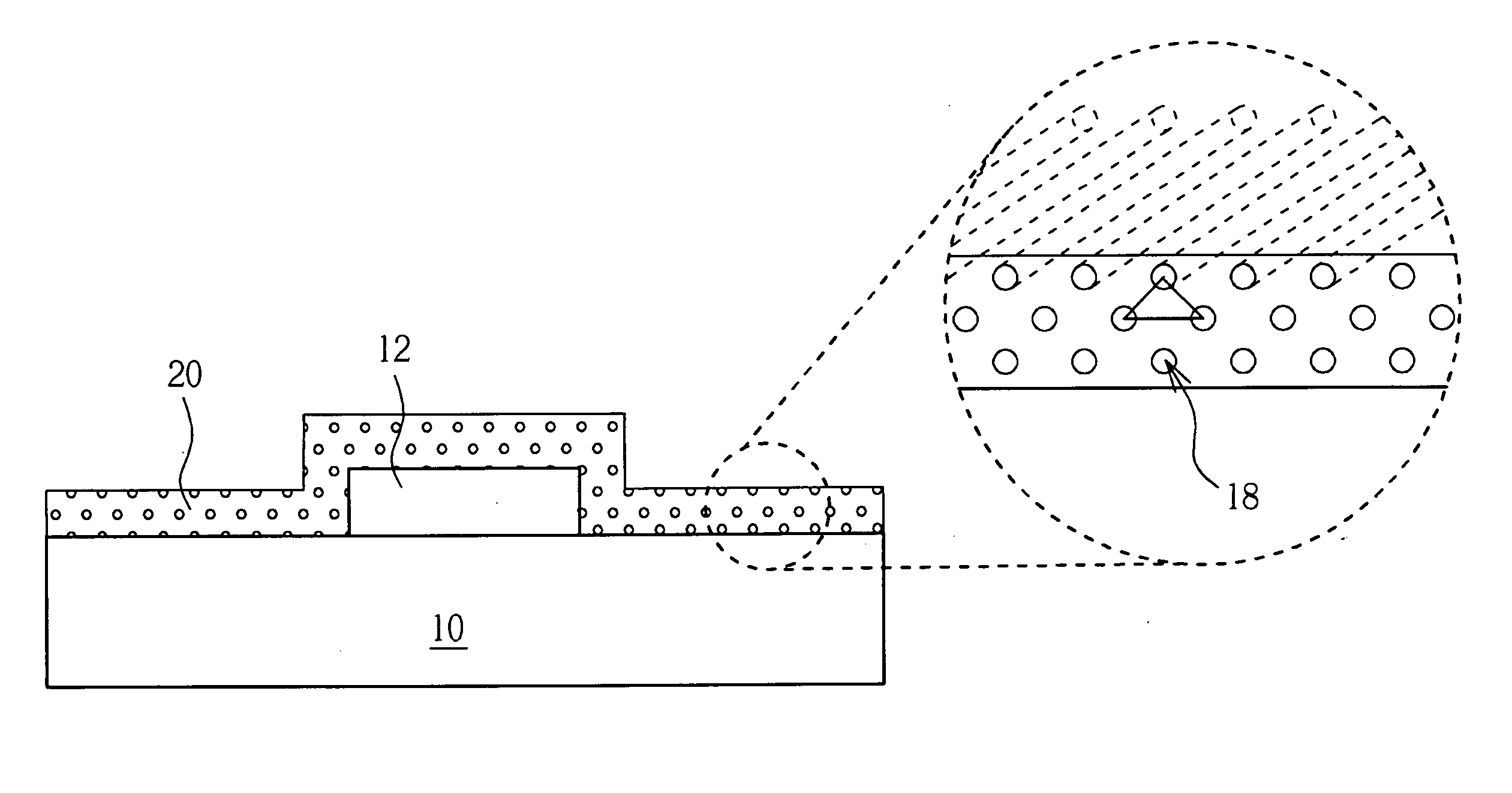
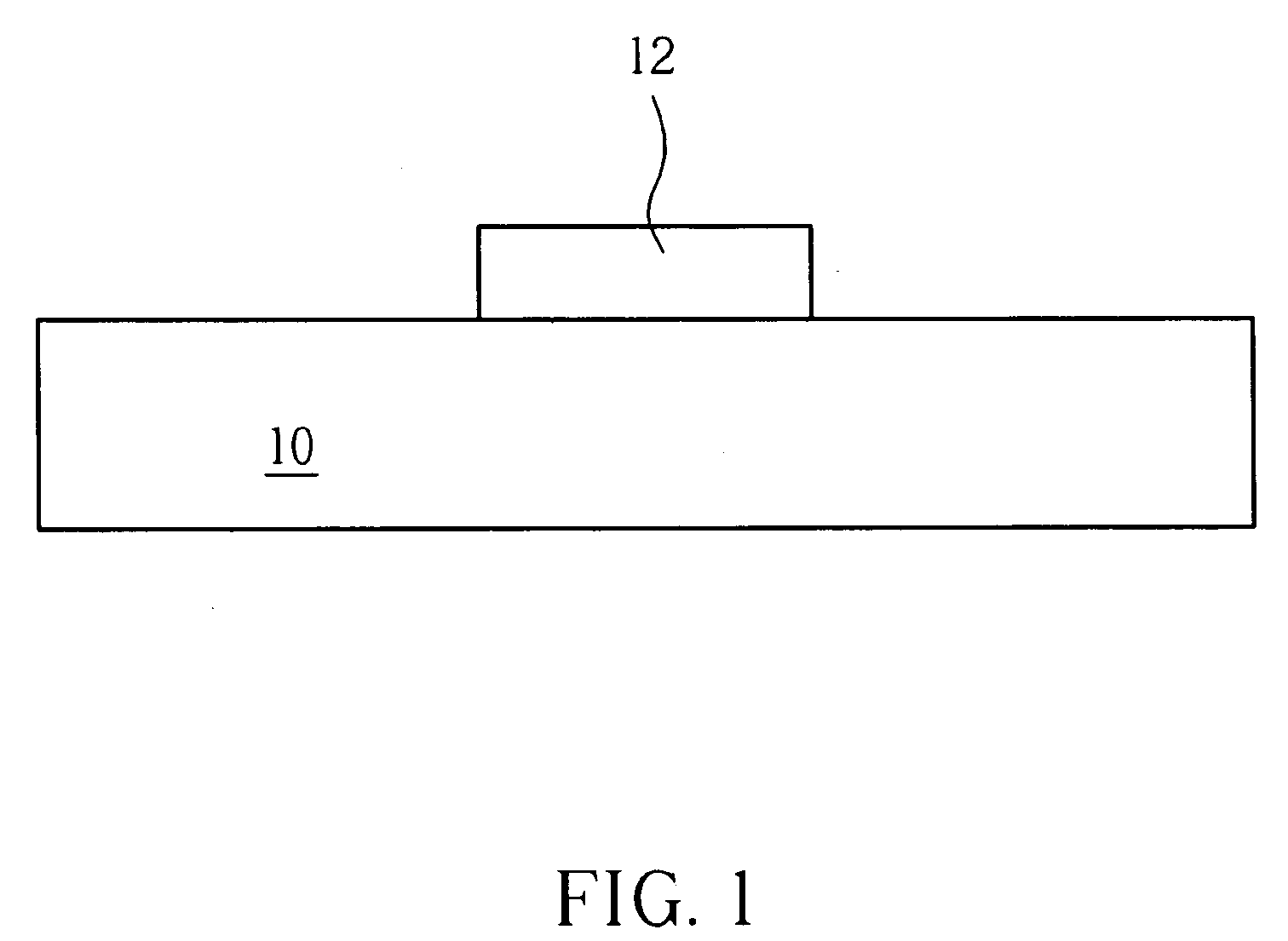
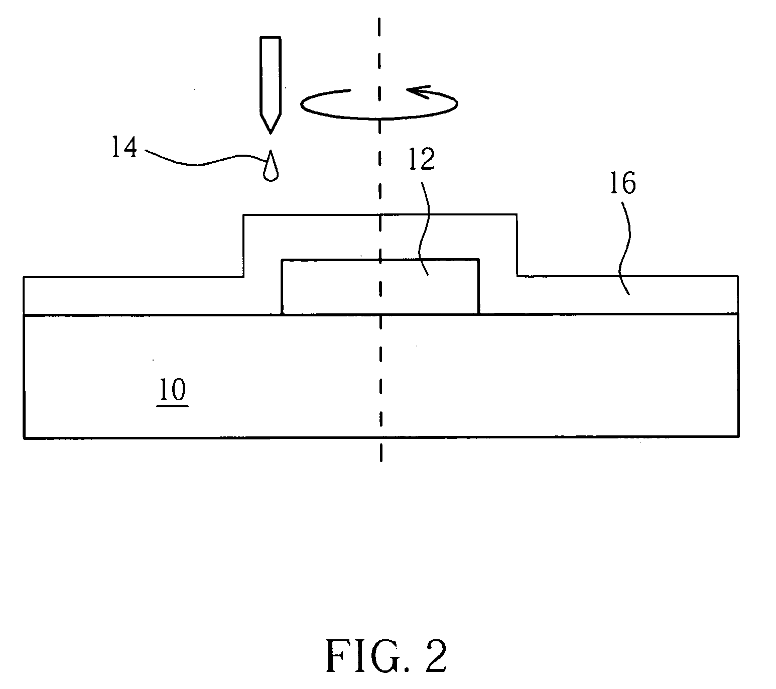
[0017]Please refer to FIG. 1 through FIG. 4. FIGS. 1 through 4 are schematic diagrams illustrating a manufacturing method of an LED device according to a first preferred embodiment of the present invention. FIG. 4 is a cross-sectional diagram illustrating an LED device according to a first preferred embodiment of the present invention. As shown in FIG. 1, the manufacturing method of the LED device of the present invention first provides a substrate 10 and at least one LED 12 disposed on the substrate 10. The substrate 10 can be a substrate, such as a circuit board, leadframe or silicon substrate etc., used for different purposes so as to hold the LED 12, but is not limited to these purposes. The LED 12 can also be an LED chip on a wafer without being cut, and the substrate 10 can also be a holder or a carrier used to perform following processes for the LED 12 on the wafer. In addition, the light emitted by the LED 12 can be any kind of color, and the wavelength of the light emitted ...


PUM

PropertyMeasurementUnit
temperatureaaaaaaaaaa
thicknessaaaaaaaaaa

Abstract

A manufacturing method of an LED device includes the following steps. First, a substrate and at least one LED disposed on the substrate are provided. Next, a porous material layer having a plurality of pores is formed on a surface of the LED. Finally, a plurality of nanocrystals are formed in the pores to construct a phosphor layer on the surface of the LED.

Description

BACKGROUND OF THE INVENTION[0001]1. Field of the Invention[0002]The present invention relates to a light emitting diode (LED) device and a manufacturing method thereof, and more particularly, to a manufacturing method that includes forming a porous material layer on an LED and disposing each pore in the porous material layer with nanocrystals, and an LED device having the nanocrystals manufactured according to the manufacturing method.[0003]2. Description of the Prior Art[0004]In general, a white LED device utilizes an LED to excite a specific phosphor material, and then mix light from both LED and phosphor material to achieve white light. However, particles sizes of the phosphor material is several micrometers, incident visible light may be shielded and scattered by phosphor powders and the luminous efficiency of the white LED device will be reduced. In order to improve this problem, a combination of an LED and nanoscale phosphor powders is utilized. Although the combination of an ...

Claims


Application Information

Patent Timeline
Patent Type & Authority Applications(United States)
IPC IPC(8): H01J1/63B05D3/00H05H1/24
CPCH01L33/501
Inventor TSAI, TZENG-GUANGSHIEH, JIA-MINKAO, CHIH-CHIANGSU, HUNG-YUAN
Owner LITE ON ELECTRONICS (GUANGZHOU) LTD
Why Eureka
Try Eureka