Organic electroluminescent device and preparation method thereof

An electroluminescent device, organic technology, applied in the direction of electric solid device, semiconductor/solid state device manufacturing, electrical components, etc., to achieve the effect of prolonging the life of the device, improving the barrier performance, and excellent packaging effect

Inactive Publication Date: 2015-04-15
OCEANS KING LIGHTING SCI&TECH CO LTD +2
View PDF0 Cites 4 Cited by
  • Summary
  • Abstract
  • Description
  • Claims
  • Application Information

AI Technical Summary

Problems solved by technology

The method of the invention is especially suitable for e

Method used


Image

  • Organic electroluminescent device and preparation method thereof
  • Organic electroluminescent device and preparation method thereof
  • Organic electroluminescent device and preparation method thereof

Examples


Embodiment 1

[0061] A method for preparing an organic electroluminescent device, comprising the following steps:

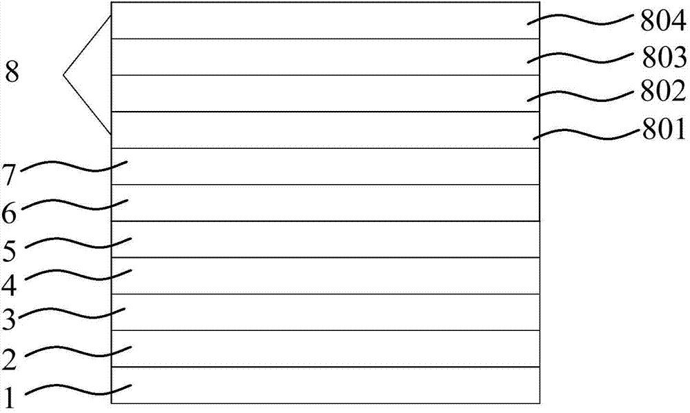
[0062] (1) Pre-treatment of ITO conductive glass substrate 1: put ITO conductive glass substrate 1 into acetone, ethanol, deionized water, and ethanol in sequence, ultrasonically clean them for 5 minutes, then blow dry with nitrogen, and dry them in an oven for later use; The cleaned ITO glass substrate 1 is subjected to surface activation treatment to increase the oxygen content of the conductive surface layer and improve the work function of the conductive layer surface; the thickness of the ITO glass substrate 1 is 100nm;

[0063] Hole injection layer 2: Evaporate MoO on the ITO conductive glass substrate 1 3 Hybrid material obtained by doping NPB, MoO 3The mass of NPB accounts for 30% of the mass of NPB, and the evaporation is carried out by high vacuum coating equipment, and the vacuum degree during evaporation is 3×10 -5 Pa, the evaporation rate is A hole injection l...

Embodiment 2

[0082] A method for preparing an organic electroluminescent device, comprising the following steps:

[0083] (1) Same as embodiment 1;

[0084] (2) Prepare an encapsulation layer on the cathode layer to obtain an organic electroluminescent device. The preparation method of the encapsulation layer is as follows:

[0085] Prepare a protective layer on the cathode layer by vacuum evaporation, the material of the protective layer is NPB, and the vacuum degree is 8×10 -5 Pa, the evaporation rate is The thickness is 300nm;

[0086] The fluoride layer is prepared by magnetron sputtering on the protective layer, and the material of the fluoride layer is HfF 4 , with a thickness of 120nm and a background vacuum of 1×10 -5 Pa;

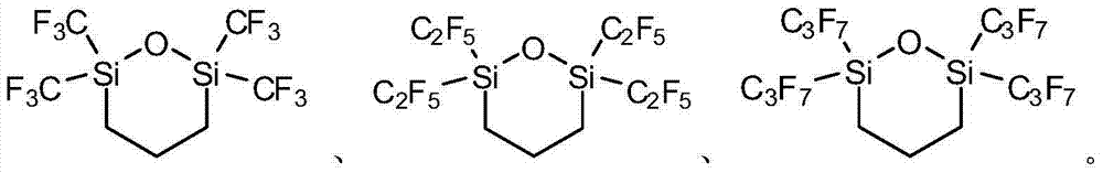
[0087] A PET film is provided, and an organic silicon layer is prepared on the PET film by first spin coating and then exposed to obtain a PET film provided with an organic silicon layer. The material of the organic silicon layer is poly[(3-(bis(pentafluor...

Embodiment 3

[0092] A method for preparing an organic electroluminescent device, comprising the following steps:

[0093] (1) Same as embodiment 1;

[0094] (2) Prepare an encapsulation layer on the cathode layer to obtain an organic electroluminescent device. The preparation method of the encapsulation layer is as follows:

[0095] The method of vacuum evaporation is used to prepare a protective layer on the cathode layer. The material of the protective layer is Alq3, and the vacuum degree is 3×10 -5 Pa, the evaporation rate is The thickness is 250nm;

[0096] The fluoride layer is prepared by magnetron sputtering on the protective layer, and the material of the fluoride layer is ZrF 4 , with a thickness of 150nm and a background vacuum of 2×10 -4 Pa;

[0097] A PET film is provided, and an organic silicon layer is prepared on the PET film by first spin coating and then exposed to obtain a PET film provided with an organic silicon layer. The material of the organic silicon layer is ...


PUM

PropertyMeasurementUnit
Thicknessaaaaaaaaaa
Thicknessaaaaaaaaaa
Thicknessaaaaaaaaaa

Abstract

The invention provides an organic electroluminescent device. The organic electroluminescent device comprises an anode conductive substrate, a cavity implantation layer, a cavity transmission layer, a luminescent layer, an electron transmission layer, an electron injecting layer, a cathode layer and a packaging layer which are successively stacked. The anode conductive substrate and the packaging layer form an enclosed space, and the cavity implantation layer, the cavity transmission layer, the luminescent layer, the electron transmission layer and the electron injecting layer and the cathode layer are accommodated in the enclosed space. The packaging layer comprises a protective layer, a fluoride layer, an organic silicon layer and a poly(ethylene terephthalate) membrane which are successively stacked. The invention further provides a preparation method of the organic electroluminescent device. According to the invention, the method can effectively reduce corrosion caused by oxygen and steam to the organic electroluminescent device, forms effective protection of the organic function material of the device and electrodes, and can substantially prolong the life of the organic electroluminescent device. The method is especially suitable for packaging a flexible organic electroluminescent device.

Description

technical field [0001] The invention relates to the related field of electronic devices, in particular to an organic electroluminescent device and a preparation method thereof. Background technique [0002] Organic electroluminescent device (OLED) is a current-mode semiconductor light-emitting device based on organic materials. Its typical structure is to prepare an organic luminescent material with a thickness of tens of nanometers on the ITO glass as a light-emitting layer, and a metal electrode with a low work function is placed above the light-emitting layer. When a voltage is applied to the electrodes, the light-emitting layer produces light radiation. [0003] OLED devices have the advantages of active luminescence, high luminous efficiency, low power consumption, lightness, thinness, and no viewing angle restrictions. They are considered by industry insiders to be the new generation of devices that are most likely to occupy a dominant position in the future lighting ...

Claims


Application Information

Patent Timeline
IPC IPC(8): H01L51/52H01L51/54H01L51/56
CPCH10K50/844H10K71/00
Inventor 周明杰钟铁涛王平陈吉星
Owner OCEANS KING LIGHTING SCI&TECH CO LTD
Why Eureka
Try Eureka