Pixel circuit, driving method of pixel circuit, display panel and display device

A technology for pixel circuits and driving transistors, applied in the fields of display panels and display devices, pixel circuits and driving methods thereof, capable of solving problems affecting the light-emitting brightness of light-emitting devices OLED and adverse effects on the display effect of AMOLED display panels, etc., so as to avoid the generation of light-emitting brightness Influence and improve the effect of display effect

Inactive Publication Date: 2015-04-29
BOE TECH GRP CO LTD +1
View PDF6 Cites 8 Cited by
  • Summary
  • Abstract
  • Description
  • Claims
  • Application Information

AI Technical Summary

Problems solved by technology

[0006] According to the above formula, the driving current for driving the light-emitting device OLED to emit light is related to the threshold voltage Vth of the driving transistor, and in practical applications, the threshold voltage Vth of the driving transistor will change during the light-emitting stage, thereby affecting the light-emitting brightness of the light-emitting device OLED. In turn, it will adversely affect the display effect of the AMOLED display panel.

Method used


Image

  • Pixel circuit, driving method of pixel circuit, display panel and display device
  • Pixel circuit, driving method of pixel circuit, display panel and display device
  • Pixel circuit, driving method of pixel circuit, display panel and display device

Examples


Embodiment Construction

[0034] The specific embodiments of the present invention will be described in detail below with reference to the accompanying drawings. It should be understood that the specific embodiments described herein are only used to illustrate and explain the present invention, and not to limit the present invention.

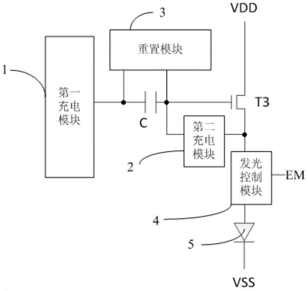
[0035] The present invention provides an embodiment of a pixel circuit, figure 1 It is a structural diagram of a pixel circuit provided by an embodiment of the present invention. Such as figure 1 As shown, the pixel circuit includes: a first charging module 1, a storage capacitor C, a second charging module 2, a reset module 3, a driving transistor T3, a light emitting control module 4, and a light emitting device 5; wherein, the first charging The module 1 and the second charging module 2 are respectively connected to both ends of the storage capacitor C for charging both ends of the storage capacitor C; the reset module 3 is connected to both ends of the storage capacitor...


PUM


Abstract

The invention relates to a pixel circuit, a driving method of the pixel circuit, a display panel and a display device. The pixel circuit comprises a first charging module, a storage capacitor, a second charging module, a resetting module, a drive transistor, an emission control module and a light-emitting device. The first charging module and the second charging module are connected with two ends of the storage capacitor, respectively and are used for charging the two ends of the storage capacitor. The resetting module is connected with the two ends of the storage capacitor and used for resetting voltages of the two ends of the storage capacitor to respective initial voltages; a control electrode of the drive transistor is connected with one end, connected with the second charging module, of the storage capacitor; a first electrode of the drive transistor is connected with a high-tension terminal, and a second electrode of the drive transistor is connected with the second charging module; the emission control module is connected between the drive transistor and the light-emitting device and used for connecting or disconnecting the drive transistor and the light-emitting device. The pixel circuit keeps lighting brightness of the light-emitting device in the displaying process, and displaying effect is thereby improved.

Description

Technical field [0001] The present invention relates to the technical field of liquid crystal display, in particular to a pixel circuit and a driving method thereof, a display panel and a display device. Background technique [0002] The Active Matrix Organic Light Emitting Diode (AMOLED) display panel uses OLED to emit light of different brightness, so that the pixels corresponding to the OLED display have corresponding brightness; compared to the traditional thin film transistor liquid crystal display panel ( Thin Film Transistor Liquid Crystal Display, hereinafter referred to as TFT LCD), AMOLED display panels have faster response speed, higher contrast and wider viewing angles, which is an important development direction of display panels. [0003] The current driving the OLED to emit light can be expressed by the following formula: [0004] I OLED = β 2 ( Vgs - Vth ) 2 [0005] Among them, Vgs is the voltage difference between the gate and the ...

Claims


Application Information

Patent Timeline
Patent Type & Authority Applications(China)
IPC IPC(8): G09G3/32G09G3/3233
CPCG09G2300/0861G09G2310/0262G09G2320/043G09G3/3233G09G2300/0819G09G2300/0842G09G2310/0251G09G2320/0233G09G2320/045
Inventor 王博玄明花张毅
Owner BOE TECH GRP CO LTD
Why Eureka
Try Eureka