COA substrate and manufacturing method thereof

A manufacturing method and substrate technology, applied in semiconductor/solid-state device manufacturing, optics, instruments, etc., can solve problems such as air bubbles affecting the display effect, and achieve the effect of improving the display effect

Active Publication Date: 2015-04-29
TCL CHINA STAR OPTOELECTRONICS TECH CO LTD
View PDF4 Cites 18 Cited by
  • Summary
  • Abstract
  • Description
  • Claims
  • Application Information

AI Technical Summary

Problems solved by technology

[0005] The purpose of the present invention is to provide a COA substrate and its manufacturing method to solve

Method used


Image

  • COA substrate and manufacturing method thereof
  • COA substrate and manufacturing method thereof
  • COA substrate and manufacturing method thereof

Examples


Example Embodiment

[0046] The description of the following embodiments refers to the attached drawings to illustrate specific embodiments that the present invention can be implemented. The directional terms mentioned in the present invention, such as "up", "down", "front", "rear", "left", "right", "in", "out", "side", etc., are for reference only The direction of the additional schema. Therefore, the directional terms used are used to describe and understand the present invention, rather than to limit the present invention. In the figure, units with similar structures are indicated by the same reference numerals.

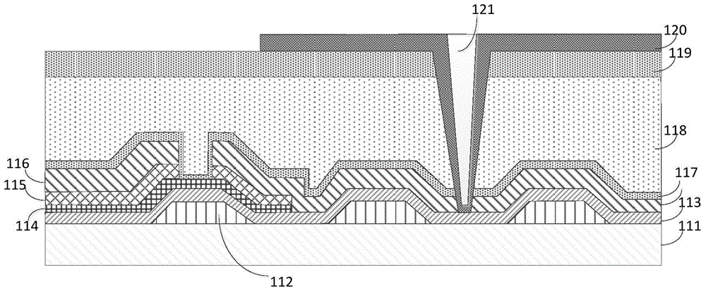
[0047] Please refer to figure 2 , figure 2 It is a schematic diagram of the structure of the COA substrate of the first embodiment of the present invention.

[0048] The COA substrate of the present invention is such as figure 2 As shown, it includes a base substrate 11, a first metal layer 12, a gate insulating layer 13, an active layer 14, an ohmic contact layer 15, a second metal l...


PUM


Abstract

The invention provides a COA substrate and a manufacturing method thereof. The method comprises the following steps: a first metal layer, a grid insulation layer, an active layer, an Ohmic contact layer, a second metal layer, a first passivation layer, a color resistance layer, a second passivation layer, a via hole and a transparent conducting layer are successively formed on a substraum substrate, wherein the first metal layer is schematized to form a grid, and the second metal layer is schematized to form a drain electrode and a source electrode; the via hole is used for connecting the pixel electrode of the transparent conducting layer to the drain electrode of the second metal layer; a spacing block and/or a black matrix is formed on the surface of the COA substrate, and the via hole is filled with organic materials of the spacing block materials or the black matrix materials. For the COA substrate and the manufacturing method thereof, disclosed by the invention, when the spacing block and/or the black matrix is formed, the via hole is filled with the spacing block materials or the black matrix materials, so that the showing effect is improved, and the production cost is reduced.

Description

【Technical field】 [0001] The invention relates to the technical field of liquid crystal displays, in particular to a COA substrate and a manufacturing method thereof. 【Background technique】 [0002] COA (Color Filter on Array) substrate is to make color filters on the array substrate, please refer to figure 1 , figure 1 It is a structural schematic diagram of a COA substrate in the prior art, such as figure 1 As shown, the existing COA substrate includes a base substrate 111, a first metal layer 112, a gate insulating layer 113, an active layer 114, an ohmic contact layer 115, a second metal layer 116, and a first passivation layer 117; The resistance layer 118, the second passivation layer 119, the transparent conductive layer 120, the transparent conductive layer 120 includes a pixel electrode, and the pixel electrode is connected to the drain of the second metal layer through the via hole 121 penetrating the color resistance layer 118 and the second passivation layer 11...

Claims


Application Information

Patent Timeline
IPC IPC(8): H01L27/12H01L21/77G02F1/1335G02F1/1333
CPCH10K59/00
Inventor 宋利旺
Owner TCL CHINA STAR OPTOELECTRONICS TECH CO LTD
Why Eureka
Try Eureka