Array substrate, display panel and display device

A technology of array substrate and display panel, applied in static indicators, instruments, etc., can solve the problems of driving transistor hysteresis and low threshold voltage, etc.

Active Publication Date: 2015-05-13
WUHAN TIANMA MICRO ELECTRONICS CO LTD +1
View PDF5 Cites 10 Cited by
  • Summary
  • Abstract
  • Description
  • Claims
  • Application Information

AI Technical Summary

Problems solved by technology

However, the transfer characteristics of the existing drive transistors are different when the gate voltage changes from positive to negative (forward scanning) and from negative to positive (reverse scanning). The threshold voltage of the transfer characteristic curve obtained by the forward scan is smaller than that of the transfer characteristic curve obtained by the forward scan, and the sub-threshold swing in the reverse scan result is smaller than the sub-threshold swing in the forward scan result, This phenomenon is the hysteresis effect of the drive transistor

Method used


Image

  • Array substrate, display panel and display device
  • Array substrate, display panel and display device
  • Array substrate, display panel and display device

Examples


Embodiment Construction

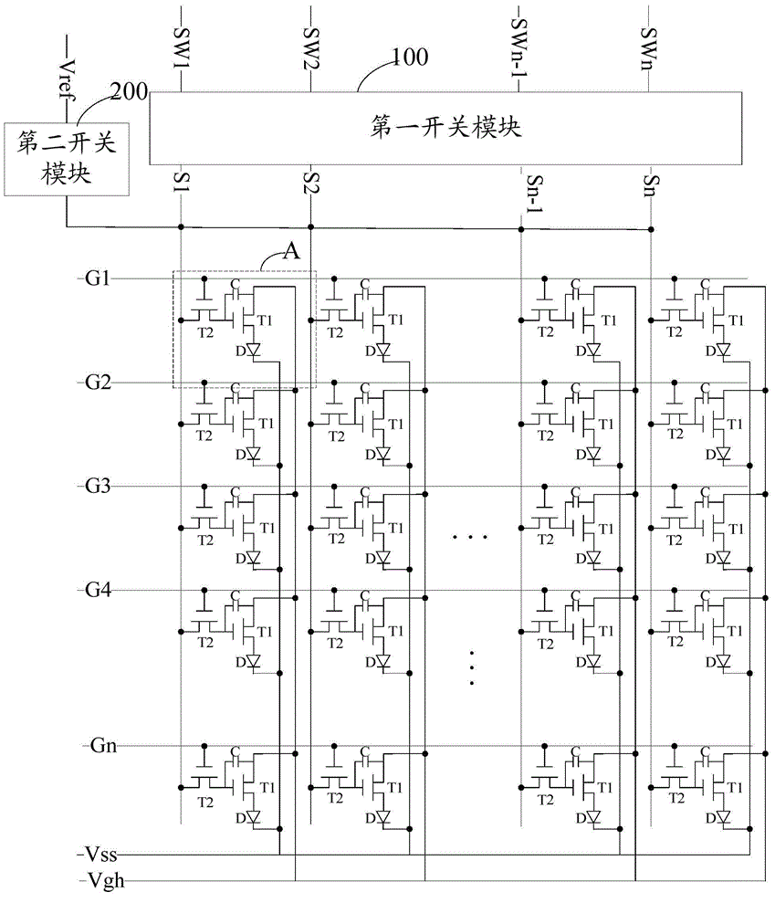
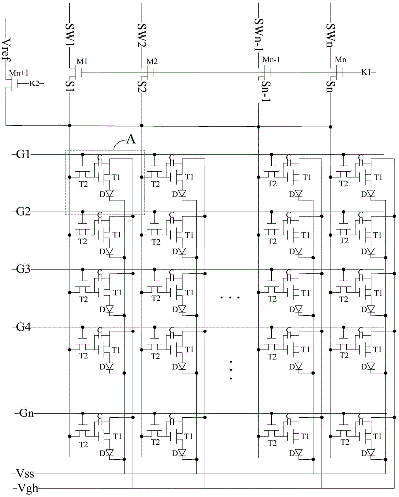
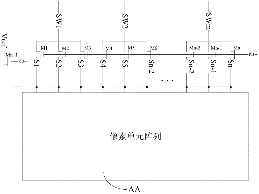
[0016] The following will be combined with the appendix in the embodiment of the present invention Figure The technical solutions in the embodiments of the present invention are described clearly and completely. Obviously, the described embodiments are only a part of the embodiments of the present invention, not all the embodiments. Based on the embodiments of the present invention, all other embodiments obtained by those of ordinary skill in the art without creative work shall fall within the protection scope of the present invention.

[0017] As mentioned in the background art, OLED (Organic Light-Emitting Diode, organic electro-laser display) display devices require the driving transistor of the pixel circuit to ensure the stability of the output current, that is, under the same gate voltage, the driving in the pixel circuit The drive current output by the transistor can maintain the sameness in time and uniformity in space. However, the transfer characteristics of the existi...


PUM


Abstract

The invention discloses an array substrate, a display panel and a display device. The array substrate comprises a substrate body, a plurality of gate lines, first to N data lines, a first switch module and a second switch module, the gate lines, the data lines, the first switch module and the second switch module are positioned on the substrate body, the first to N data lines and the gate lines are intersected to form a pixel unit array, a pixel unit comprises a driving transistor and a light-emitting diode, a first end of the driving transistor is connected to a high-potential signal, a second end of the driving transistor is connected to a positive electrode of the light-emitting diode, an input end of the first switch module is connected to a corresponding data signal, an output end of the first switch module is connected to corresponding input ends of the first to N data lines, an input end of the second switch module is connected to a reset signal, an output end of the second switch module is connected to the first to N data lines, and ghost shadows caused by retardation effects of the driving transistor are avoided when the display device displays frames.

Description

technical field [0001] The present invention relates to the field of display technology, and more specifically, to an array substrate, a display panel and a display device. Background technique [0002] The OLED (Organic Light-Emitting Diode, organic electro-laser display) display device requires the driving transistor of the pixel circuit to be able to ensure the stability of the output current, that is, under the same gate voltage, the driving current output by the driving transistor in the pixel circuit can be Maintain temporal identity and spatial uniformity. However, the transfer characteristics of existing drive transistors are different when the gate voltage changes from positive to negative (forward scanning) and from negative to positive (reverse scanning). The threshold voltage of the transfer characteristic curve obtained by the forward scan is smaller than that of the transfer characteristic curve obtained by the forward scan, and the sub-threshold swing in the ...

Claims


Application Information

Patent Timeline
Patent Type & Authority Applications(China)
IPC IPC(8): G09G3/32G09G3/3208
Inventor 张成凤孔祥梓吕博嘉
Owner WUHAN TIANMA MICRO ELECTRONICS CO LTD
Why Eureka
Try Eureka