Multiplexing gate drive circuit and display panel

A gate drive circuit and multiplexing technology, which is applied in the direction of static indicators, digital memory information, instruments, etc., can solve the problem of insufficient opening of thin film transistors, poor release of residual charges on the display panel, residual image on the display panel, etc. problem, achieve the effect of reducing threshold consumption, improving effect, and preventing afterimage phenomenon

Inactive Publication Date: 2020-12-01
WUHAN CHINA STAR OPTOELECTRONICS TECH CO LTD
View PDF3 Cites 2 Cited by
  • Summary
  • Abstract
  • Description
  • Claims
  • Application Information

AI Technical Summary

Problems solved by technology

When the existing MOG circuit implements the AllGate On function, the gate drive signal G(n) output by each level of GOA unit is divided by the multiplexing circuit. The amplitude of the m sub-gate drive signals is low, resulting in a low The thin-film transistors of the pixels in the display are not fully turned on, and the residual charge release effect of the display panel is poor, which may cause image sticking on the display panel during the wake-up phase of the black screen.

Method used


Image

  • Multiplexing gate drive circuit and display panel
  • Multiplexing gate drive circuit and display panel
  • Multiplexing gate drive circuit and display panel

Examples


Embodiment Construction

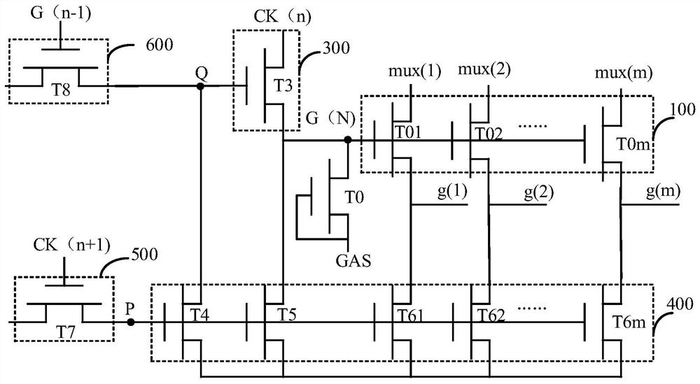
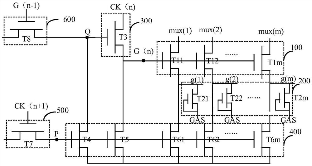
[0023] The technical solutions in the embodiments of the present application will be clearly and completely described below in conjunction with the drawings in the embodiments of the present application. Apparently, the described embodiments are only some of the embodiments of this application, not all of them. Based on the embodiments in this application, all other embodiments obtained by those skilled in the art without making creative efforts belong to the scope of protection of this application.

[0024] In all embodiments of the present application, in order to distinguish the two poles of the TFT except the gate, one pole is called the source, and the other pole is called the drain. Since the source and drain of a thin film transistor are symmetrical, their source and drain are interchangeable. According to the form in the attached drawing, it is stipulated that the middle terminal of the thin film transistor is the gate, the signal input terminal is the source, and the...


PUM


Abstract

The invention provides a multiplexing gate drive circuit and a display panel. According to the multiplexing gate drive circuit, when the All Gate On function is carried out on a GOA circuit by adopting a multiplexing module, the multiplexing gate drive circuit can be used for driving the GOA circuit; the multiplexing module divides the gate driving signal G(n) into sub-gate driving signals g(1)-g(m), and the output amplitude values are relatively low, and the problem of poor function of the Al<l> Gate On is solved; a full-open control module is improved to be respectively connected with sub-gate drive signals g (1)-g(m) segmented by each gate drive signal G(n); the full-open control module can directly control each sub-gate drive signal g(1)-g(m) to output high potential at the same time;and in this way, only one time of threshold value consumption is needed from the full-open control signal to the sub-grid driving signal, the final action potential of the full-open control signal canbe improved, the effect of the All Gate On function is effectively improved, and the ghost phenomenon is prevented from occurring when the display panel is awakened in a black screen mode.

Description

technical field [0001] The present application relates to the field of display technology, in particular to a multiplexing gate drive circuit and a display panel. Background technique [0002] GOA (Gate Driver On Array) technology integrates the gate driver circuit of the display panel on the glass substrate to form a scanning drive for the display panel. GOA technology can reduce the bonding process of external ICs and reduce product costs. It is suitable for Make narrow bezel display products. [0003] The multiplexing (Demultiplexer, DEMUX) circuit can decompose a signal into m signal channels, thereby reducing the output channels exponentially, and applying the multiplexing circuit to the gate drive circuit is called MOG (Mux on Gate) technology, which can further realize the narrow frame of the display panel. Therefore, the MOG technology can be applied to the GOA circuit, that is, the gate drive signal G(n) output by the clock signal from each level of GOA unit is di...

Claims


Application Information

Patent Timeline
Patent Type & Authority Applications(China)
IPC IPC(8): G09G3/20
CPCG09G3/20G09G2320/0257G11C19/28G09G2300/0408G09G2310/0267G09G2310/08G09G2310/0297G09G2310/0286G09G2300/0804G09G2300/0809
Inventor 张典戴荣磊
Owner WUHAN CHINA STAR OPTOELECTRONICS TECH CO LTD
Why Eureka
Try Eureka