A pixel circuit, its driving method, display panel, and display device

A pixel circuit, drive control technology, applied in the field of pixel circuits, display panels and display devices, can solve the problems of inconsistent brightness of the first frame, achieve consistent brightness, avoid voltage jumps, and avoid effects of parasitic capacitance

Active Publication Date: 2019-06-28
WUHAN TIANMA MICRO ELECTRONICS CO LTD +1
View PDF5 Cites 2 Cited by
  • Summary
  • Abstract
  • Description
  • Claims
  • Application Information

AI Technical Summary

Problems solved by technology

[0004] Embodiments of the present invention provide a pixel circuit, its driving method, a display panel, and a display device, which are used to improve the afterimage existing in the existing pixel circuit and the problem of inconsistency in brightness of the first frame after switching between high and low gray scales

Method used


Image

  • A pixel circuit, its driving method, display panel, and display device
  • A pixel circuit, its driving method, display panel, and display device
  • A pixel circuit, its driving method, display panel, and display device

Examples


example 1

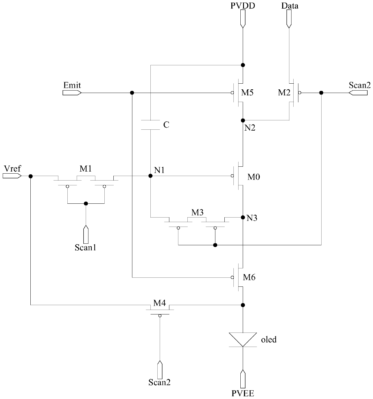
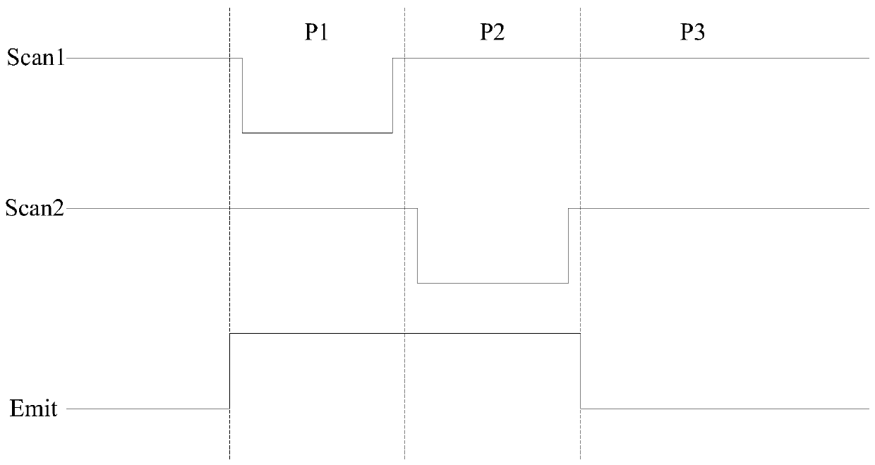
[0101] by Figure 5 Take the pixel circuit shown as an example, all switching transistors are P-type transistors, and the corresponding input and output timings are as follows: Figure 9 shown. Specifically, select Figure 9 The four stages T1, T2, T3 and T4 in the input timing diagram shown.

[0102] In the T1 stage (that is, the initialization stage 1), Scan1=0, Scan2=1, Scan3=1, Emit=0.

[0103] Since Scan1=0, the fourth switching transistor M4 is turned on, and the signal of the first voltage terminal PVDD is transmitted to the first node N1 through the fourth switching transistor M4, so the potential of the first node N1 is VDD. Since Emit=0, the fifth switching transistor M5 and the sixth switching transistor M6 are turned on. The signal of the first voltage terminal PVDD is transmitted to the second node N2 through the fifth switch transistor M5, so the potential of the second node N2 is VDD. The first node N1 and the second node N2 are at the same potential. Beca...

example 2

[0112] by Figure 8 Take the pixel circuit shown as an example, all switching transistors are N-type transistors, and the corresponding input and output timings are as follows Figure 10 shown. Specifically, select Figure 10 The four stages T1, T2, T3 and T4 in the input timing diagram shown.

[0113] In the T1 stage (that is, the initialization stage 1), Scan1=1, Scan2=0, Scan3=0, Emit=1.

[0114]Since Scan1=1, the fourth switching transistor M4 is turned on, and the signal of the first voltage terminal PVDD is transmitted to the first node N1 through the fourth switching transistor M4, so the potential of the first node N1 is VDD. Since Emit=1, the fifth switching transistor M5 and the sixth switching transistor M6 are turned on. The signal of the first voltage terminal PVDD is transmitted to the second node N2 through the fifth switch transistor M5, so the potential of the second node N2 is VDD. The first node N1 and the second node N2 are at the same potential. Beca...


PUM


Abstract

The invention discloses a pixel circuit, a driving method thereof, a display panel and a display device. A node reset module is used to provide a signal of a first voltage terminal to a gate of a driving transistor before a driving control module controls a driving transistor to drive a light-emitting device to emit light; At the same time, when the node reset module supplies the signal of the first voltage terminal to the gate of the driving transistor, the light emission control module supplies the signal of the first voltage terminal to the first electrode of the driving transistor. That is, before the light-emitting device emits light, the signal of the first voltage terminal is used to reset the gate and the first electrode of the driving transistor at the same time, so as to avoid the difference caused by the parasitic capacitance of the two, and thus avoid the problem of inconsistent threshold value capture caused by voltage jumps , which can ensure that the brightness of the first frame is consistent after switching between high and low gray levels. In addition, the drive transistor is completely reset in the initialization phase of each frame, which can also prevent the image sticking phenomenon caused by the shift of the threshold voltage of the drive transistor.

Description

technical field [0001] The invention relates to the field of display technology, in particular to a pixel circuit, a driving method thereof, a display panel and a display device. Background technique [0002] Organic Light Emitting Diode (OLED) is one of the hot spots in the field of flat panel display research today. Compared with liquid crystal displays, OLED has the advantages of low energy consumption, low production cost, self-illumination, wide viewing angle and fast response speed. , OLEDs have begun to replace traditional Liquid Crystal Displays (LCDs) in the field of flat panel displays such as mobile phones, PDAs, and digital cameras. Among them, pixel circuit design is the core technical content of OLED display, which has important research significance. [0003] The structure of an existing pixel circuit is as follows figure 1 As shown, it includes 6 switch transistors: M1-M6, 1 drive transistor M0 and 1 capacitor C. The corresponding input timing diagram is a...

Claims


Application Information

Patent Timeline
Patent Type & Authority Patents(China)
IPC IPC(8): G09G3/3208
CPCG09G3/3208G09G3/3233G09G2300/0819G09G2310/0216G09G2320/045G09G2300/0842G09G2320/0257G09G3/3291G09G2320/0233G09G2320/043H01L27/1251H01L29/78645H01L29/78696
Inventor 高娅娜向东旭朱仁远李玥陈泽源蔡中兰
Owner WUHAN TIANMA MICRO ELECTRONICS CO LTD
Why Eureka
Try Eureka