Semiconductor device

a semiconductor and device technology, applied in semiconductor devices, diodes, electrical devices, etc., can solve the problems of increasing the number of parts, the potential connection between the gate resistance and the semiconductor chip is liable to change, and the semiconductor device is liable to malfunction or oscillate, etc., to achieve high reliability, small footprint, and large current

Active Publication Date: 2008-11-27
MITSUBISHI ELECTRIC CORP
View PDF24 Cites 22 Cited by
  • Summary
  • Abstract
  • Description
  • Claims
  • Application Information

AI Technical Summary

Benefits of technology

[0012]An object of the invention is to provide a semiconductor device having a resistance element that has a small footprint and can pass a large current with high reliability.

Problems solved by technology

The above semiconductor device having the external gate resistance suffers from a problem of increase in number of parts.
Also, a potential of connection between the gate resistance and the semiconductor chip is liable to change due to external noises, and this potential change directly affects the gate in the semiconductor chip without mediation of a gate resistance.
This results in a problem that the semiconductor device is liable to malfunction or oscillate.
However, increase in thickness results in problems that a long time is required for depositing a film forming the internal gate resistance, and that processing or working of the film thus deposited is difficult.
Also, increase in width results in a problem that areas of the internal gate resistance and therefore the semiconductor chip increase.

Method used


Image

  • Semiconductor device
  • Semiconductor device
  • Semiconductor device

Examples


first embodiment

[0082]First, a schematic structure of a semiconductor device of a first embodiment will be described.

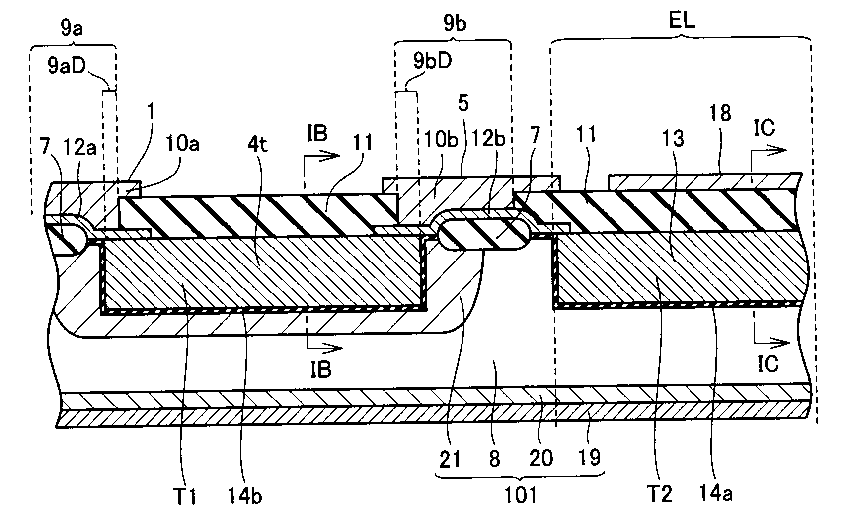
[0083]Referring to FIGS. 1A-1C, an IGBT chip of this embodiment is a power semiconductor device, and has an IGBT element EL that is a trench gate type semiconductor element, and a trench type internal gate resistance 4t that is a resistance element.

[0084]Referring to FIGS. 1A and 1B, trench type internal gate resistance 4t is formed in a first trench T1 formed at a semiconductor substrate 101 with an insulating film 14b therebetween. Thereby, trench type internal gate resistance 4t is configured such that a sectional area of its current path increases with increase in depth of first trench T1.

[0085]Referring to FIGS. 1A and 1C, IGBT element EL has a channel region formed of a part of semiconductor substrate 101. IGBT element EL has a large number of gate electrodes 13 for controlling the channel region. Gate electrodes 13 are, e.g., hundreds to tens of thousands in number.

[0086]Refer...

second embodiment

[0146]First, a structure of a IGBT chip that is a semiconductor device of a second embodiment will be described.

[0147]Referring to FIGS. 21-24, the IGBT chip of this embodiment has a metal portion 22. Metal portion 22 includes metal portions 22b1 and 22b2 arranged inside first trench T1, and a metal portion 22a arranged inside second trench T2. A material of metal portion 22 has a lower resistivity than a semiconductor material such as heavily doped n-type polycrystalline silicon. The material of metal portion 22 is, e.g., high-melting point metal such as tungsten, titanium, platinum or copper.

[0148]Referring to FIG. 24, gate electrode 13 has a polycrystalline silicon layer 12g, and metal portion 22a filling a space inside polycrystalline silicon layer 12g.

[0149]Referring to FIGS. 22 and 23, trench type internal gate resistance 4t has buried metal portion 22b1 in a portion opposed to gate pad side contact hole 9aD. Also, trench type internal gate resistance 4t has buried metal port...

third embodiment

[0190]First, a structure of an IGBT chip that is a semiconductor device of a third embodiment will be described.

[0191]Referring to FIG. 39, trench type internal gate resistance 4t that is a resistance element of the semiconductor device of this embodiment includes, as a major element, an n-type lightly doped polycrystalline silicon layer 23a. Trench type internal gate resistance 4t has an n-type heavily doped polycrystalline silicon layer 24a located in portions that are in contact with gate pad side contact hole 9a and main interconnection side contact hole 9b.

[0192]The semiconductor device of this embodiment differs from those of the first and second embodiments in that a major portion of the buried substance of trench type internal gate resistance 4t is the polycrystalline silicon layers of a lower concentration than those in the first and second embodiments, and the potential difference between trench type internal gate resistance 4t and p-type region 21 in contact with it can ...


PUM


Abstract

A semiconductor device has a semiconductor substrate, an insulating film, a semiconductor element and a resistance element. The semiconductor substrate has a first trench. The insulating film covers an inner surface of the first trench. The semiconductor element has an electrode. The resistance element is electrically connected to the electrode to form a resistance to a current flowing through the electrode, and is arranged in the first trench with the insulating film therebetween. Thereby, the semiconductor device can have a resistance element that has a small footprint and can pass a large current with high reliability.

Description

BACKGROUND OF THE INVENTION[0001]1. Field of the Invention[0002]The present invention relates to a semiconductor device, and particularly to a semiconductor device including a channel region formed of a part of a semiconductor substrate and an electrode.[0003]2. Description of the Background Art[0004]As semiconductor devices, there are power semiconductor chips such as an IGBT (Insulated Gate Bipolar Transistor) and a power MOSFET (Metal Oxide Semiconductor Field-Effect Transistor). Gates of these semiconductor chips primarily have a plane gate structure or a trench gate structure.[0005]In the prior art, the gate of the trench gate structure is made of, e.g., polycrystalline silicon. In recently years, such a method has been proposed that uses metal of a high melting point for lowering a resistivity of the trench gate. According to, e.g., Japanese Patent Laying-Open No. 2001-044435, a polycrystalline silicon layer, i.e., a buffer layer as well as high-melting point metal are formed ...

Claims


Application Information

Patent Timeline
Patent Type & Authority Applications(United States)
IPC IPC(8): H01L27/06
CPCH01L27/0611H01L2924/0002H01L29/1095H01L29/4232H01L29/42356H01L29/4238H01L29/66333H01L29/7395H01L29/7803H01L29/7804H01L29/7808H01L29/7813H01L29/0696H01L2924/00H01L29/70H01L29/73
Inventor KUSUNOKI, SHIGERUMOCHIZUKI, KOICHIKAWAKAMI, MINORU
Owner MITSUBISHI ELECTRIC CORP
Why Eureka
Try Eureka