Pixel structure and display panel

A technology of pixel structure and pixel electrode, applied in nonlinear optics, instruments, optics, etc., can solve the problems of liquid crystal molecules toppling, affecting the light transmittance of the display panel, etc., and achieve the effect of improving the light transmittance

Inactive Publication Date: 2018-04-27
AU OPTRONICS CORP
View PDF5 Cites 0 Cited by
  • Summary
  • Abstract
  • Description
  • Claims
  • Application Information

AI Technical Summary

Problems solved by technology

However, liquid crystal molecules will experience different electric field magnitudes and directions under the action of a non-uniform electric field, causing some liquid crystal molecules to fall in unexpected directions, and produce undesired dislocation lines ( disclination line) and disclination node, which in turn affect the light transmittance of the display panel

Method used


Image

  • Pixel structure and display panel
  • Pixel structure and display panel
  • Pixel structure and display panel

Examples


Embodiment Construction

[0065] The present invention will be described in detail below in conjunction with the accompanying drawings and specific embodiments, but not as a limitation of the present invention.

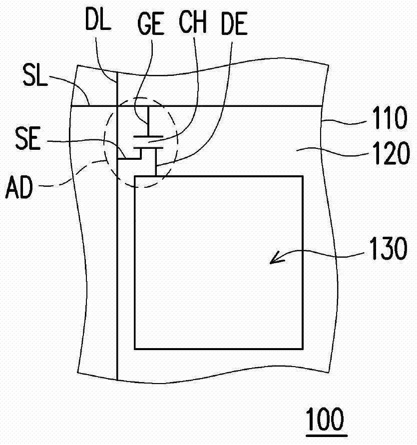
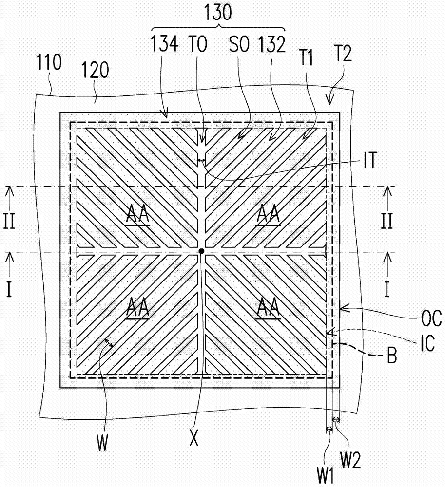
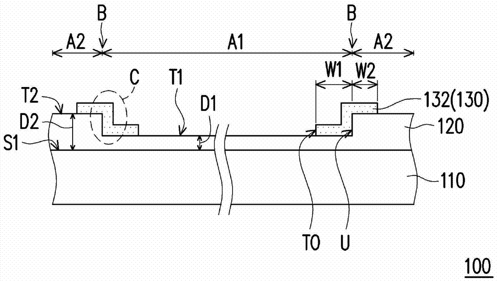
[0066] Figure 1A It is a schematic top view of a pixel structure according to an embodiment of the present invention. Figure 1B yes Figure 1A A partially enlarged schematic diagram of an embodiment of the pixel structure. Figure 1C and Figure 1D are along Figure 1B The cross-sectional schematic diagram of the section line I-I, II-II. Please refer to Figure 1A to Figure 1D , the pixel structure 100 includes a substrate 110 , an insulating layer 120 and a pixel electrode 130 . The substrate 110 can be a glass substrate, a silicon substrate, a flexible plastic substrate, or any known substrate that can be used in making display panels. The substrate 110 has a surface S1. The insulating layer 120 and the pixel electrode 130 are disposed on the surface S1, and the insulating layer 120 ...


PUM


Abstract

The invention discloses a pixel structure, comprising a substrate with surfaces, an insulating layer, and pixel electrodes. The insulating layer defines a first region and a second region surrounding the first region. The first region is provided with a first region top surface and the second region is provided with a second region top surface. A first distance from the first region top surface to the surface is smaller than a second distance from the second region top surface to the surface. The pixel electrode continuously extends from the first region top surface to the second region top surface, wherein the pixel electrode is provided with a backbone opening and a plurality of slit openings communicated with the backbone opening. The backbone opening is distributed along a cross track, so as to mark off a plurality of alignment regions. The slit openings in a same alignment region are parallel to each other, and a stripe portion of the pixel electrode is defined between two adjacent slit openings. The intersected position of the cross track is in the first region. Also provided is a display panel.

Description

technical field [0001] The present invention relates to a pixel structure and a display panel, and in particular to a pixel structure that helps to improve light transmittance and a display panel using the pixel structure. Background technique [0002] Currently, the performance requirements of the market for LCD panels include high contrast ratio, no gray scale inversion, low color shift, high luminance, and high color saturation. , quick response and wide viewing angle. At present, the technologies that can meet the requirement of wide viewing angle include Twisted Nematic (TN) liquid crystal with wide viewing film (wide viewing film), in-plane switching (In-Plane Switching, IPS) liquid crystal display panel, marginal field switching Type (Fringe Field Switching) liquid crystal display panel, multi-domain vertical alignment (Multi-domain Vertical Alignment, MVA) liquid crystal display panel, etc. [0003] In the existing multi-domain vertical alignment liquid crystal dis...

Claims


Application Information

Patent Timeline
Patent Type & Authority Patents(China)
IPC IPC(8): G02F1/1343G02F1/1362
CPCG02F1/133345G02F1/1343G02F1/139
Inventor 李益志叶昭纬古正彬郑伟成丁天伦林贞君
Owner AU OPTRONICS CORP
Why Eureka
Try Eureka