
Small-sized chip type surface mounting (SMD) high-voltage and safety standard recognized ceramic capacitor

A ceramic capacitor, surface mount technology, applied in the direction of fixed capacitor dielectric, fixed capacitor shell/package, fixed capacitor components, etc., can solve the problem of not being suitable, and achieve cost saving, small size, high electric strength Effect

Inactive Publication Date: 2015-06-10
鞍山奇发电子陶瓷科技有限公司
View PDF11 Cites 11 Cited by
  • Summary
  • Abstract
  • Description
  • Claims
  • Application Information

AI Technical Summary

Benefits of technology

This patented technical effect of this innovation relates to making better quality electronic components by reducing their sizes while maintaining their functionality. It achieves these benefits through use of specialized chips that have improved properties such as higher voltage ratings or less expensive material compared to older designs. These improvements result from reduced manufacturing costs without sacrificing reliability due to smaller dimensions.

Problems solved by technology

This patented technical problem addressed in this patents relates to improving upon conventional methods used during electronics assembly that require large amounts of space due to their bulky design or requiring expensive material processing techniques like sintered metal powders.

Method used


Image

  • Small-sized chip type surface mounting (SMD) high-voltage and safety standard recognized ceramic capacitor
  • Small-sized chip type surface mounting (SMD) high-voltage and safety standard recognized ceramic capacitor
  • Small-sized chip type surface mounting (SMD) high-voltage and safety standard recognized ceramic capacitor

Examples


Embodiment Construction

[0028] The specific embodiment of the present invention is further described below in conjunction with accompanying drawing:

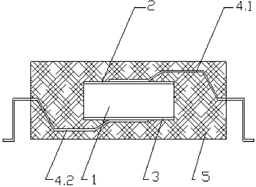
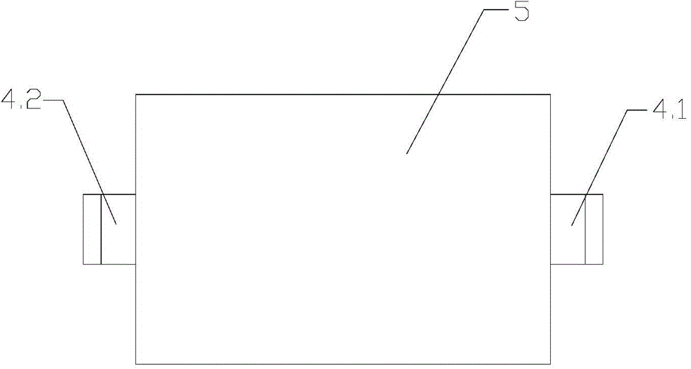
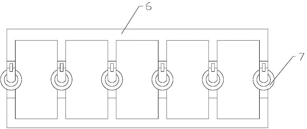
[0029] Such as figure 1 , figure 2 As shown, a surface mount type ceramic safety capacitor includes a copper electrode ceramic chip, a steel strip pin 4 and an epoxy resin encapsulation material 5, the copper electrode ceramic chip is a cylinder, and the ceramic dielectric 1 is located on the upper and lower electrodes 2, In the middle of 3, the upper and lower electrodes 2 and 3 are integral copper electrodes, the upper electrode 2 and the upper steel strip pin 4.1 are welded and fixed, the lower electrode 3 and the lower steel strip pin 4.2 are welded and fixed, and the epoxy resin encapsulation material 5 wraps the copper electrode The ceramic chip and a part of the steel strip pin 4 are encapsulated together, and the end of the steel strip pin 4 is exposed outside the epoxy resin encapsulation material 5 .

[0030] The manufacturing method of th...


PUM


Abstract

The invention relates to a small-sized hip type surface mounting (SMD) high-voltage and safety standard recognized ceramic capacitor and a manufacturing method thereof. The capacitor comprises holosymmetrical copper electrode ceramic chips, a copper belt pin and an encapsulating material, wherein the holosymmetrical copper electrode ceramic chips are cylindrical; a ceramic medium is positioned between upper and lower electrodes which are integral copper electrodes; the copper belt pin is welded and fixed with the upper and lower electrodes; the encapsulating material is used for encapsulating the copper electrode ceramic chips and one part of the copper belt pin together, and the tail end of the copper belt pin is exposed out of the encapsulating material. The manufacturing method for the capacitor comprises the following steps: inserting chips, welding, vacuum injection-molding and encapsulating epoxy resin, curing and molding at a high temperature, laser-printing product performance information and safety certification information, cutting a pin, performing full-automatic performance test, taping and packaging a reel. The capacitor has the characteristics of being stable in capacity, high in electric strength and small in size, effectively saves the surface space of a PCB (printed circuit board), and is suitable for existing small-sized and ultrathin requirements of a whole circuit of an electrical appliance product, so that the market needs are met.

Description


Claims


Application Information

Patent Timeline
Owner 鞍山奇发电子陶瓷科技有限公司
Learn More