

Post-treatment method for removing photoresist and manufacturing method of semiconductor device
A production method and photoresist technology, applied in semiconductor/solid-state device manufacturing, electrical components, circuits, etc., can solve the problem that wet cleaning is difficult to meet the requirements of the surface cleanliness of semiconductor devices
- Summary
- Abstract
- Description
- Claims
- Application Information
AI Technical Summary
Problems solved by technology
Method used
Image

Examples
Embodiment 1
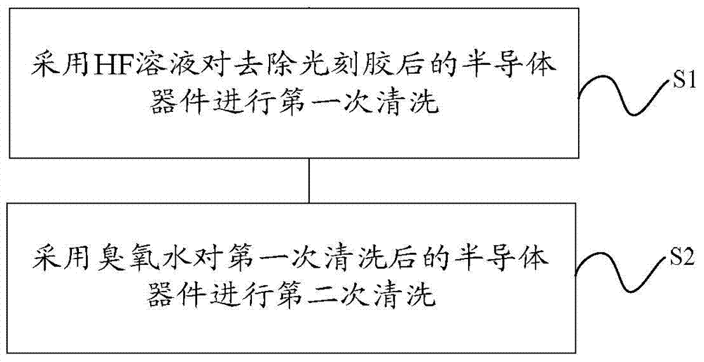
[0037] This embodiment provides a post-processing method for photoresist removal, comprising the following steps:
[0038] The semiconductor device after removing the photoresist is cleaned for the first time, and its specific steps include: at 20 ° C, HF and H 2 The HF solution with the volume ratio of O of 1:500 is sprayed onto the semiconductor device after the first cleaning, and the HF solution is evenly distributed on the surface of the semiconductor device by rotating at a low speed (300rpm), and the flow rate of the HF solution is 1.2L / min; The semiconductor device after removing the photoresist is cleaned for the first time, and the cleaning time is 60 seconds.
[0039] Carry out the second cleaning to the semiconductor device after cleaning for the first time, its specific steps include: at 20 ℃, the O 3 The ozone water with a content of 10ppm is sprayed onto the semiconductor device after the first cleaning, and the ozone water is evenly distributed on the surface ...
Embodiment 2
[0042] This embodiment provides a post-processing method for photoresist removal, comprising the following steps:
[0043] The semiconductor device after removing the photoresist is cleaned for the first time, including the following steps: at 30 ° C, HF and H 2 The HF solution with a volume ratio of O of 1:1600 is placed in a cleaning tank, and then the semiconductor device after removing the photoresist is immersed in the HF solution for cleaning, and the cleaning time is 45 seconds.
[0044] Carry out the second cleaning to the semiconductor device after the first cleaning, its specific steps include: at 30 ℃, the O 3 The ozone water with a content of 55ppm is sprayed on the semiconductor device after the first cleaning, and the ozone water is evenly distributed on the surface of the semiconductor device by rotating at a low speed (300rpm). The flow rate of the ozone water is 1.2L / min; for the first The second cleaning is performed on the semiconductor device after the fir...
Embodiment 3
[0047] This embodiment provides a post-processing method for photoresist removal, comprising the following steps:
[0048] The semiconductor device after removing the photoresist is cleaned for the first time, and its specific steps include: at room temperature, HF and H 2 The HF solution with a volume ratio of O of 1:3000 is sprayed on the semiconductor device after the first cleaning, and the HF solution is evenly distributed on the surface of the semiconductor device by rotating at a low speed (500rpm), and the flow rate of HF is 2L / min; The semiconductor device after removing the photoresist is cleaned for the first time, and the cleaning time is 5 seconds.
[0049] Carry out the second cleaning to the semiconductor device after cleaning for the first time, its specific steps include: at room temperature, the O 3 The ozone water with a content of 100ppm is sprayed on the semiconductor device after the first cleaning, and the ozone water is evenly distributed on the surfac...
PUM
 Abstract
Description
Claims
Application Information