Low-temperature and shock-resistant semiconductor package structure

A packaging structure and semiconductor technology, applied in semiconductor devices, semiconductor/solid-state device components, electric solid-state devices, etc., can solve the problems of large size and inertia of high-power chips, and achieve low operating temperature rise and extended service life. Effect

Active Publication Date: 2015-07-08
KUNSHAN POLYSTAR ELECTRONICS
View PDF6 Cites 3 Cited by
  • Summary
  • Abstract
  • Description
  • Claims
  • Application Information

AI Technical Summary

Problems solved by technology

However, despite this, some high-power chips are still relatively large in size, and their inertia is also relatively large. In h

Method used


Image

  • Low-temperature and shock-resistant semiconductor package structure

Examples


Embodiment Construction

[0011] The present invention will be further described in detail below in conjunction with the accompanying drawings and specific embodiments.

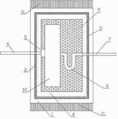
[0012] Such as figure 1 As shown, a low-temperature shock-resistant semiconductor packaging structure includes a functional device, a packaging layer and a heat sink 11, the packaging layer wraps and covers the functional device, and the functional device includes a large-area contact piece 5, a semiconductor device 10, a micro tension U U-shaped conductive shrapnel 8 and elastic thermally conductive colloid 9, the elastic thermally conductive colloid 9 wraps and covers the large-area contact piece 5, the semiconductor device 10 and the micro-tension U-shaped conductive shrapnel 8, and the large-area contact piece 5 is electrically connected to the semiconductor device 10, The semiconductor device 10 is electrically connected to the micro-tension U-shaped conductive elastic piece 8, the large-area contact piece 5 is electrically conne...


PUM


Abstract

The invention discloses a low-temperature and shock-resistant semiconductor package structure which comprises a functional device, a packaging layer and a cooling and heat conduction device. According to the scheme, direct stress of the packaging layer will not be borne by a chip, so the chip can bear high shake stress; in addition, thanks to auxiliary heat dissipation of heat dissipation fins and quick heat conduction of elastic heat conduction colloids, it can be guaranteed that a semiconductor product is in a low operating temperature rise state.

Description

technical field [0001] The invention relates to the technical field of semiconductor packaging, in particular to a low-temperature shock-resistant semiconductor packaging structure. technical background [0002] In terms of semiconductor packaging technology, some semiconductor chips are still in a relatively high power state in order to meet the needs of use, especially with the update and progress of technology, semiconductor chips are gradually becoming smaller and smaller to meet market demand. . However, despite this, some high-power chips are still relatively large in size, and their inertia is also relatively large. In high-vibration situations, the impact on the safety of the chip is more obvious. Heat dissipation brings certain negative effects. Therefore, it is necessary to provide a semiconductor packaging structure that can maintain a low-temperature state during product operation and is highly shock-resistant. Contents of the invention [0003] The inventio...

Claims


Application Information

Patent Timeline
IPC IPC(8): H01L23/16H01L23/29H01L23/367H01L23/552
Inventor 卢涛张小平
Owner KUNSHAN POLYSTAR ELECTRONICS
Why Eureka
Try Eureka