Substrate detection system
A substrate detection and substrate technology, which is applied in the direction of measuring electricity, measuring devices, measuring electrical variables, etc., can solve problems such as the inability to meet the competitive needs of rapid and high-quality production, and achieve the effect of improving detection efficiency
- Summary
- Abstract
- Description
- Claims
- Application Information
AI Technical Summary
Problems solved by technology
Method used
Image


Examples
no. 1 example 〕
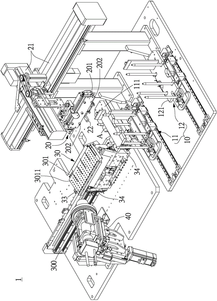
[0089] Please also refer to Figure 1 to Figure 7 , which is a schematic diagram of the first embodiment of the substrate inspection system of the present invention. Such as figure 1 As shown, the substrate inspection system 1 includes: a loading device 10 , a carrying device 20 , a first substrate adsorption stage 30 and a first inspection device 40 . The material placement device 10 includes a first substrate placement area 11 and a second substrate placement area 12; for example, the first substrate placement area 11 can place the substrate A to be detected, and the second substrate placement area 12 It may be to place the inspected substrate A, and in practical application, it may be based on the detection result of the first inspection device 40 to design, for example, a substrate re-inspection area, a substrate damage area, and the like. The first substrate placement area 11 and the second substrate placement area 12 can be respectively provided with a movable platform...
no. 2 example
[0102] Please also refer to Figure 8 and Figure 9 , which is a schematic diagram of the second embodiment of the substrate inspection system of the present invention. Such as Figure 8 As shown, the substrate detection system 2 includes: a material placement device 10, a carrier device 20, a first substrate adsorption stage 30, a first detection device 40, a second substrate adsorption stage 50, and a substrate turnover device 60 and a second detection device 70 . The relevant connection relationship of the material placement device 10 , the carrying device 20 , the first substrate adsorption stage 30 and the first detection device 40 is the same as that of the foregoing embodiments, so no further description is given here. This embodiment specifically illustrates that the substrate inspection system 2 may further include a second guide rail 500 arranged parallel to the first guide rail 300, and the second substrate adsorption carrier 50 is movably arranged on the second ...
PUM
 Abstract
Description
Claims
Application Information
 - R&D
- Intellectual Property
- Life Sciences
- Materials
- Tech Scout
- Unparalleled Data Quality
- Higher Quality Content
- 60% Fewer Hallucinations
Browse by: Latest US Patents, China's latest patents, Technical Efficacy Thesaurus, Application Domain, Technology Topic, Popular Technical Reports.
© 2025 PatSnap. All rights reserved.Legal|Privacy policy|Modern Slavery Act Transparency Statement|Sitemap|About US| Contact US: help@patsnap.com