Array substrate, display panel and display device

An array substrate and color film substrate technology, applied in the display field, can solve the problems of coupling interference between touch leads and gate lines, affecting the display effect of the display panel, etc., and achieve the effect of avoiding overlap and reducing the display effect

Active Publication Date: 2018-07-03
SHANGHAI AVIC OPTOELECTRONICS +1
View PDF6 Cites 0 Cited by
  • Summary
  • Abstract
  • Description
  • Claims
  • Application Information

AI Technical Summary

Problems solved by technology

[0004] In view of this, the present invention provides an array substrate, a display panel and a display device to solve the problem in the prior art that the display effect of the display panel is affected due to the coupling interference between the touch lead and the gate line

Method used


Image

  • Array substrate, display panel and display device
  • Array substrate, display panel and display device
  • Array substrate, display panel and display device

Examples


Embodiment Construction

[0026] The following will clearly and completely describe the technical solutions in the embodiments of the present invention with reference to the accompanying drawings in the embodiments of the present invention. Obviously, the described embodiments are only some, not all, embodiments of the present invention. Based on the embodiments of the present invention, all other embodiments obtained by persons of ordinary skill in the art without making creative efforts belong to the protection scope of the present invention.

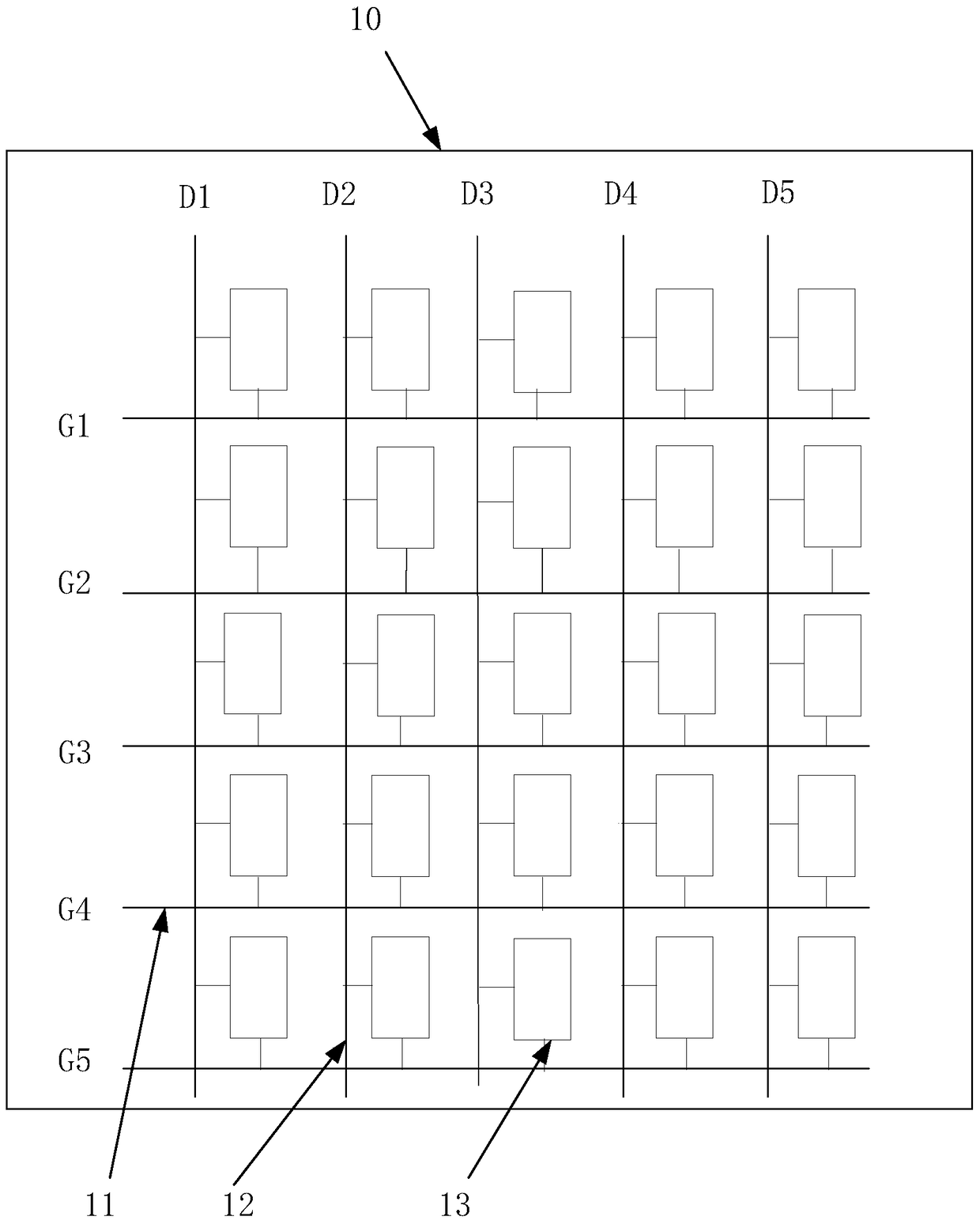
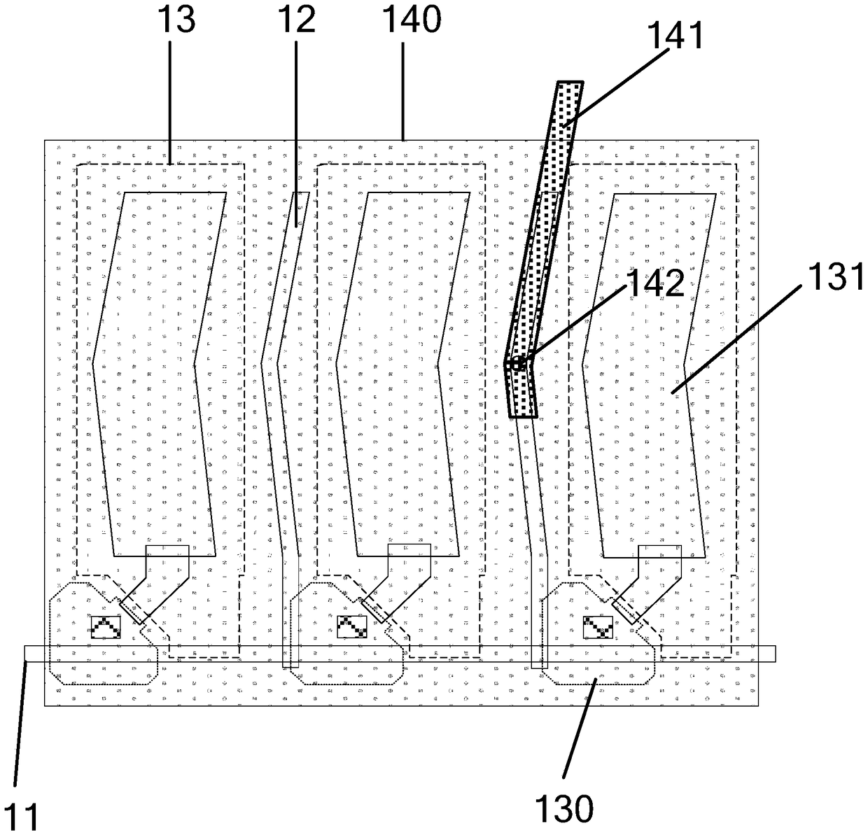
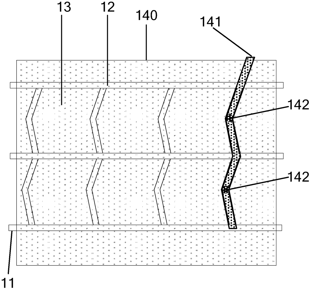
[0027] An embodiment of the present invention provides an array substrate, referring to figure 1 and figure 2 , figure 1 It is a schematic structural diagram of an array substrate provided in an embodiment of the present application, figure 2 for figure 1 A partially enlarged view of an embodiment of the array substrate shown.

[0028] The array substrate includes a substrate 10, a plurality of gate lines 11 and a plurality of data lines 12 arranged on t...


PUM


Abstract

The invention provides an array substrate, a display panel and a display device. The array substrate comprises a substrate, multiple grid electrode lines, multiple data lines, a common electrode layer and a lead-wire layer, wherein the grid electrode lines and the data lines are arranged at the same side of the substrate, the grid electrode lines intersect with the data lines, so that multiple pixel units are limited out, each pixel unit comprises pixel electrodes, and each pixel electrode is a strip-shaped electrode provided with one or more corners; the common electrode layer is arranged to be opposite to the pixel electrodes in the direction perpendicular to the substrate, and the common electrode layer comprises multiple touch-control electrodes; the lead-wire is arranged to be opposite to the common electrode layer in the direction perpendicular to the substrate, and the lead-wire layer comprises multiple touch-control lead wires which are connected with the touch-control electrodes; each touch-control lead wire is in electric connection with the corresponding touch-control electrode through one or more via holes; the via holes are located at the corners of the pixel electrodes, so that overlapping of the via holes of the touch-control lead wires and the grid electrode lines is avoided, and the problem that the display effect of the display panel is affected by coupling of the touch-control lead wires and the grid electrode lines is reduced.

Description

technical field [0001] The present invention relates to the field of display technology, and more specifically, to an array substrate, a display panel and a display device. Background technique [0002] The touch display device integrating the touch panel and the display panel has become the most widely used touch display device at present due to the advantages of reducing the use of substrates and being lighter and thinner. Generally, a touch display device includes an on-cell structure and an in-cell structure, wherein the in-cell structure embeds the touch panel function into pixels, and the on-cell structure embeds the touch panel function into the color filter between the sheet and the polarizer. [0003] For a touch display device with an in-cell structure, it is necessary to divide the common electrodes of the display panel into individual touch electrodes. Input touch signal and common voltage signal. However, since the via holes connecting the touch leads and the...

Claims


Application Information

Patent Timeline
Patent Type & Authority Patents(China)
IPC IPC(8): G02F1/1362G02F1/1343
CPCG02F1/13338G02F1/134309G02F1/136227G02F1/136286G02F2201/123
Inventor 金慧俊
Owner SHANGHAI AVIC OPTOELECTRONICS
Why Eureka
Try Eureka