Method for manufacturing a display device and display device

A technology for a display device and a manufacturing method, which is applied in the directions of instruments, nonlinear optics, optics, etc., can solve the problems of poor hole digging accuracy of polarizers, low processing efficiency, poor display effect of display devices, etc., to avoid the hole digging process, The effect of increasing the penetration rate

Active Publication Date: 2021-10-08
XIAMEN TIANMA MICRO ELECTRONICS
View PDF7 Cites 0 Cited by
  • Summary
  • Abstract
  • Description
  • Claims
  • Application Information

AI Technical Summary

Problems solved by technology

[0003] At present, it is possible to dig holes in the polarizer corresponding to the area where the camera is installed to meet the light transmittance requirements of the camera. However, after the polarizer, display panel, and cover plate are assembled into a module, water vapor in the air can easily pass through. The hole-digging position of the polarizer enters the inside of the display device, which affects the polarization performance of the polarizer, resulting in poor display effect of the display device
In addition, the hole-digging process of the polarizer is divided into stamping process and laser process. The stamping process requires mechanical cutting, resulting in poor hole-digging accuracy of the polarizer, while the laser process can only process one polarizer at a time, and the processing efficiency is low. , mass production cannot be achieved, and both processes increase the difficulty of digging holes for polarizers

Method used


Image

  • Method for manufacturing a display device and display device
  • Method for manufacturing a display device and display device
  • Method for manufacturing a display device and display device

Examples


Embodiment Construction

[0034] The present invention will be further described in detail below in conjunction with the accompanying drawings and embodiments. It should be understood that the specific embodiments described here are only used to explain the present invention, but not to limit the present invention. In addition, it should be noted that, for the convenience of description, only some structures related to the present invention are shown in the drawings but not all structures. Throughout this specification, the same or similar reference numerals represent the same or similar structures, elements or processes. It should be noted that, in the case of no conflict, the embodiments in the present application and the features in the embodiments can be combined with each other.

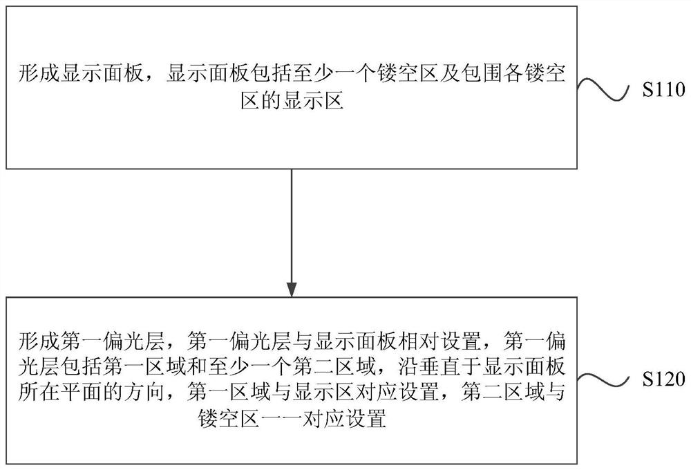
[0035] figure 1 It is a schematic flowchart of a manufacturing method of a display device provided by an embodiment of the present invention. Such as figure 1 As shown, the manufacturing method of the display device ...


PUM

PropertyMeasurementUnit
diameteraaaaaaaaaa

Abstract

The invention discloses a manufacturing method of a display device and the display device. The manufacturing method of the display device includes forming a display panel, the display panel includes at least one hollow area and a display area surrounding each hollow area; forming a first polarizing layer, a first polarizing The layer includes a first region and at least one second region. Along the direction perpendicular to the plane where the display panel is located, the first region is arranged corresponding to the display region, and the second region is arranged in one-to-one correspondence with the hollow region; forming the first polarizing layer includes A base is doped with a dichroic organic dye to form a first pre-polarizing layer; the first shielding structure is correspondingly arranged above each second region; the first pre-polarizing layer is irradiated with ultraviolet light, and the first shielding structure shields the ultraviolet light from being irradiated to each second zone. Through the technical solution of the present invention, the light transmittance of the first polarizing layer in the second region is greatly improved, and the problem of affecting the display effect of the display device by water vapor caused by punching holes in the first polarizing layer is avoided.

Description

technical field [0001] Embodiments of the present invention relate to the field of display technology, and in particular, to a method for manufacturing a display device and a display device. Background technique [0002] In order to reduce the thickness of the module of the display device, it is currently possible to open a hole in the display screen of the display device and arrange the camera in the hole area of ​​the display screen. For a display device equipped with a polarizer, such as a liquid crystal display device, in order to prevent insufficient light received by the camera from affecting the camera function of the display device, it is necessary to ensure the light transmittance of the area where the camera is installed on the display device. [0003] At present, it is possible to dig holes in the polarizer corresponding to the area where the camera is installed to meet the light transmittance requirements of the camera. However, after the polarizer, display panel...

Claims


Application Information

Patent Timeline
Patent Type & Authority Patents(China)
IPC IPC(8): G02F1/1335G02F1/1333
CPCG02F1/1333G02F1/133528
Inventor 方丽婷宋琼吴玲沈柏平
Owner XIAMEN TIANMA MICRO ELECTRONICS
Why Eureka
Try Eureka