Liquid crystal display device
A technology of a liquid crystal display device and a liquid crystal layer, which is applied in the direction of nonlinear optics, instruments, optics, etc., can solve problems such as the decline in the display quality of liquid crystal display devices, achieve excellent viewing angle characteristics, and avoid finger pressure marks
- Summary
- Abstract
- Description
- Claims
- Application Information
AI Technical Summary
Problems solved by technology
Method used
Image

Examples
Embodiment 1
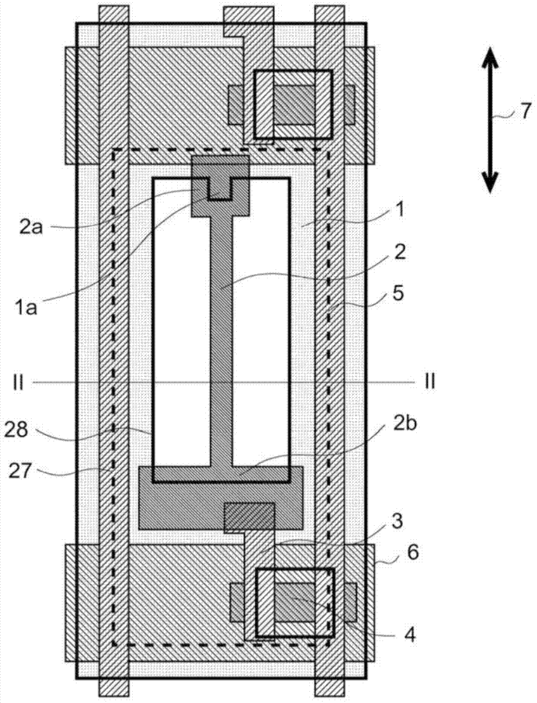
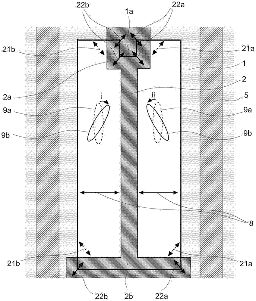
[0061] will now refer to Figure 1 to Figure 4 An exemplary liquid crystal display device according to Embodiment 1 is described. figure 1 is a plan view showing the structure of one pixel of the liquid crystal display device according to Embodiment 1, in which a unit pixel 27 is indicated by a region surrounded by a dotted line. figure 2 is the edge of the liquid crystal display device figure 1 A cross-sectional view taken along the line II-II shown in , and also shows the liquid crystal layer and the opposite substrate. image 3 yes figure 1 A zoomed-in view of the columns and their surroundings shown in . Figure 4 yes image 3 A further enlarged view of the upper and lower parts of the pixels in .
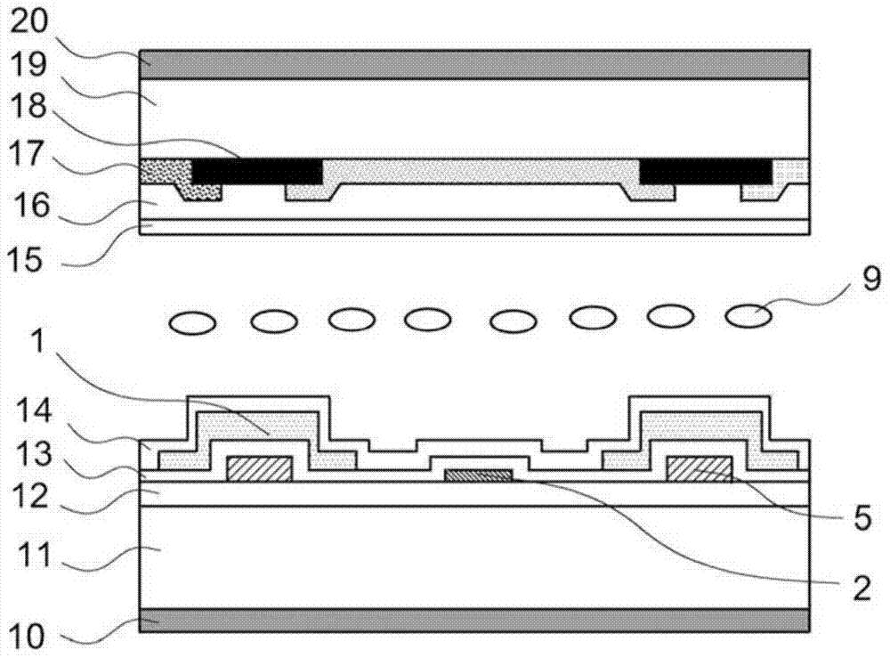
[0062] will now be described in detail Figure 1 to Figure 4 An exemplary liquid crystal display device according to Example 1 shown in . The liquid crystal display device comprises a first transparent insulating substrate 11, a second transparent insulating substrat...
Embodiment 2
[0085] will now use Figure 5 , Figure 6 and Figure 7 Example 2 is described. Figure 5 is a plan view showing the structure of one pixel of the liquid crystal display device according to Embodiment 2, in which a unit pixel 27 is indicated by a region surrounded by a dotted line. Figure 6 is along Figure 5 A cross-sectional view taken along the line VI-VI shown in , and further shows the liquid crystal layer and the opposite substrate. Figure 7 is showing Figure 6 A zoomed-in view of a column and its surroundings within a pixel in . will now be described in detail Figure 5 , Figure 6 and Figure 7 Example 2 shown in .
[0086] In Example 1, as for example figure 1 As shown, the pixel electrode is formed of a transparent conductive film. Meanwhile, in embodiment 2, such as Figure 5 , Figure 6 and Figure 7 As shown, the pixel electrode is formed by the second metal layer. That is, during the process of forming the second metal layer, the data line 5 , ...
Embodiment 3
[0088] will now use Figure 8 , Figure 9 and Figure 10 Example 3 is described. Figure 8 is a plan view showing the structure of one pixel of the liquid crystal display device according to Embodiment 3, in which a unit pixel 27 is indicated by a region surrounded by a dotted line. Figure 9 is showing Figure 8 An enlarged view of the area around data line 5 in . Figure 10 is a plan view showing a modified structure of one pixel when the portion of the common electrode covering the data line is not hollowed out, where the unit pixel 27 is indicated by a region surrounded by a dotted line. will now be described in detail Figure 8 , Figure 9 and Figure 10 Example 3 shown in .
[0089] In Embodiment 1, in each pixel, the strip-shaped pixel electrodes 2 are arranged such that the extending direction thereof is parallel to the extending direction of the data lines 5 . Meanwhile, in embodiment 3, such as Figure 8 As shown, in each pixel, the strip-shaped pixel elect...
PUM
| Property | Measurement | Unit |
|---|---|---|
| Thickness | aaaaa | aaaaa |
| Thickness | aaaaa | aaaaa |
Abstract
Description
Claims
Application Information