Signal processing device, signal processing method, imaging element, and imaging device

A signal processing device and signal technology, which are applied to electrical components, picture signal generators, image communication, etc., can solve the problems of large kTC noise, deterioration of image quality, and difficulty in fully suppressing kTC noise.

Active Publication Date: 2019-10-22
SONY SEMICON SOLUTIONS CORP
View PDF3 Cites 0 Cited by
  • Summary
  • Abstract
  • Description
  • Claims
  • Application Information

AI Technical Summary

Problems solved by technology

[0005] In particular, in the case where full depletion is not performed in the pixel structure of the imaging element, kTC noise becomes larger, and it is more difficult to sufficiently suppress kTC noise
As a result, further deterioration of the image quality of the captured image obtained by the imaging element may occur

Method used


Image

  • Signal processing device, signal processing method, imaging element, and imaging device
  • Signal processing device, signal processing method, imaging element, and imaging device
  • Signal processing device, signal processing method, imaging element, and imaging device

Examples


no. 1 example

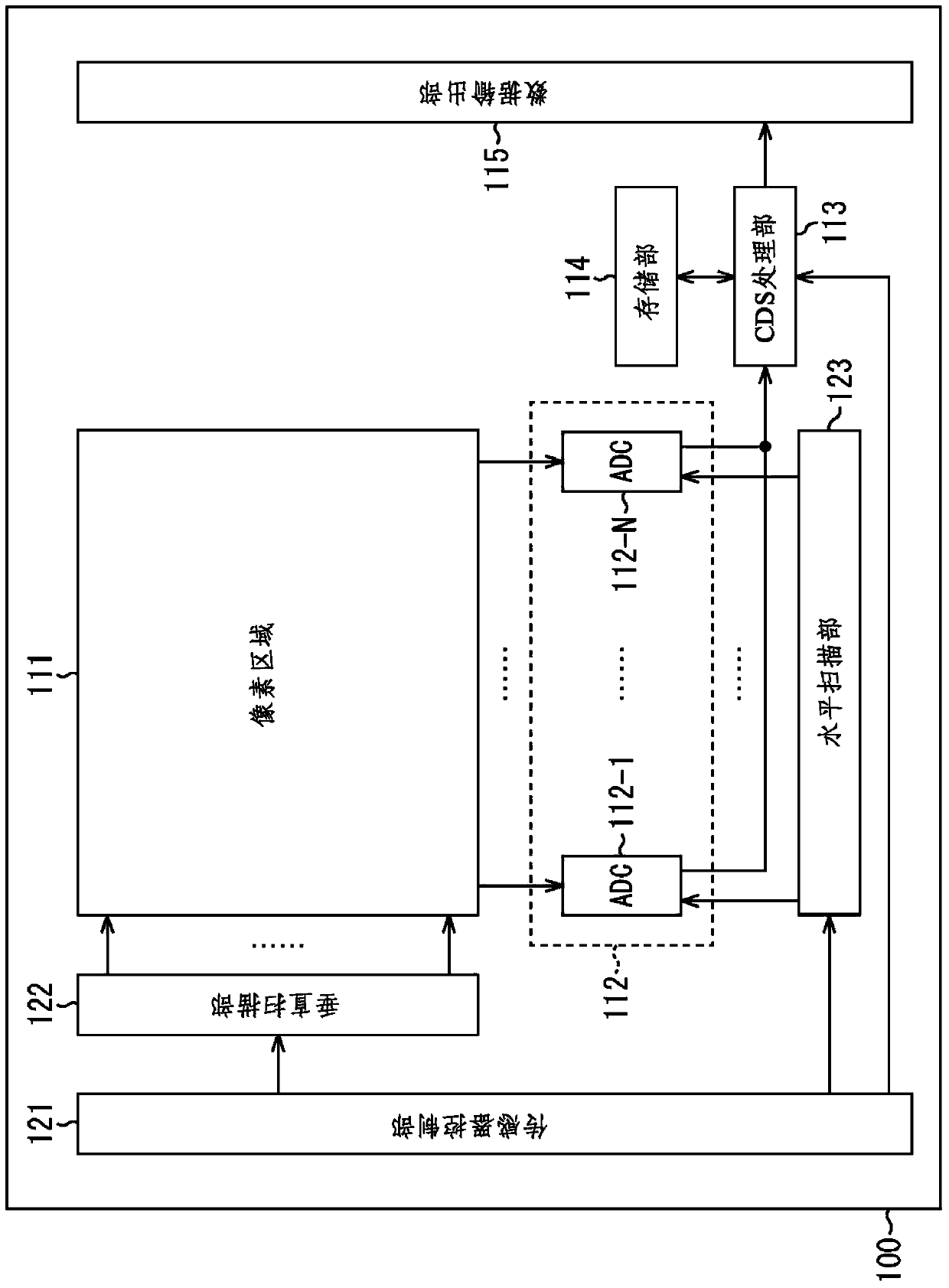
[0055] 1. First Embodiment (Signal Processing Device, Imaging Element, and Imaging Device)

[0056] 2. Second embodiment (imaging element)

no. 3 example

[0057] 3. Third embodiment (imaging element)

no. 4 example

[0058] 4. Fourth embodiment (imaging element)

[0059] 5. Fifth embodiment (imaging device)

[0060] 1. The first embodiment
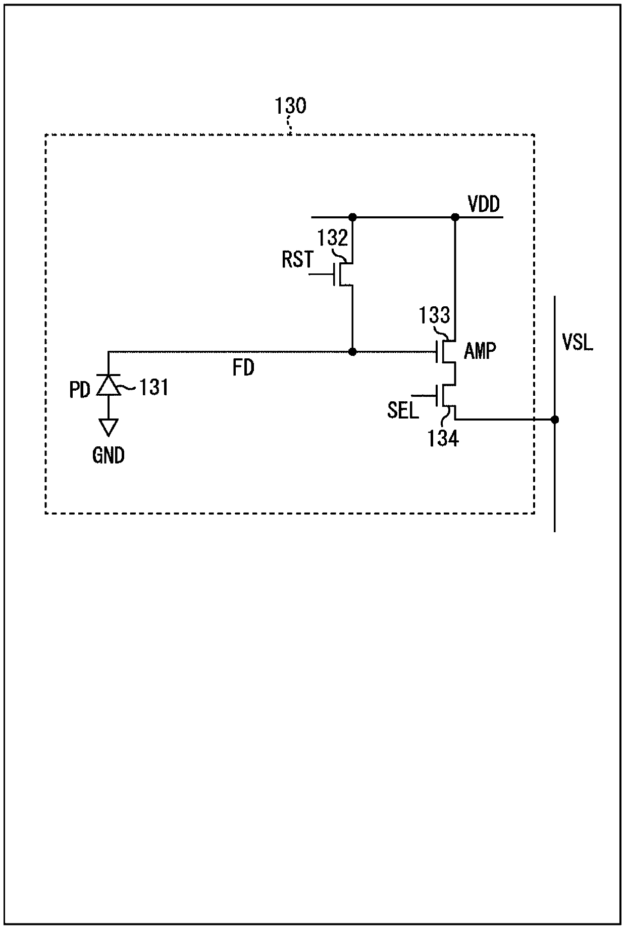
[0061] kTC noise

[0062] In recent years, image sensors (image pickup elements) using CCDs (Charge Coupled Devices) or CMOS (Complementary Metal Oxide Semiconductors) have been used as image pickup elements that pick up images in image pickup devices such as video cameras and digital still cameras. Also, as these imaging elements, single-plate type imaging elements have been used.

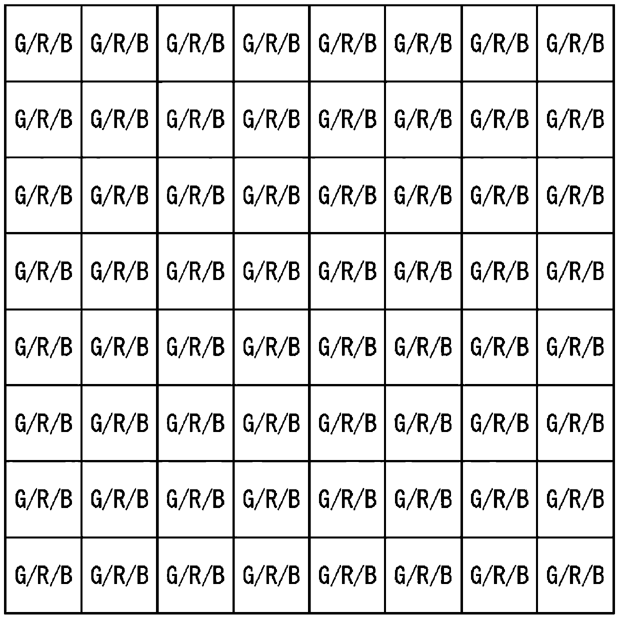
[0063] In a single-plate type image pickup element, color filters each having a different color are correspondingly provided in pixels (generally, an RGB Bayer array has been widely used). For example, where the color filters in this Bayer array have primary colors, blue and red light will not be transmitted to the pixels below the green filter. Thus, there is a problem that light cannot be used efficiently. Also, processing (demosaic processing) to generate a color i...


PUM


Abstract

The present invention relates to a signal processing device and method, an imaging element and an imaging device. The signal processing device includes: an A / D conversion section for performing A / D conversion of the first signal, A / D conversion of the second signal, A / D conversion of the third signal, and A / D conversion of the fourth signal conversion; and a correlated double sampling processing section for generating a first output signal by performing correlated double sampling using the first and second digital data items, generating a second output signal by performing correlated double sampling using the third and fourth digital data items output signal, and generate a third output signal by performing correlated double sampling using the first and second output signals, the first digital data item obtained by A / D conversion of the first signal, the second digital data The item is obtained through the A / D conversion of the second signal, the third digital data item is obtained through the A / D conversion of the third signal, and the fourth digital data item is obtained through the A / D conversion of the fourth signal. D conversion obtained. The present invention can suppress deterioration of image quality.

Description

technical field [0001] The present technology relates to a signal processing device, a signal processing method, an imaging element, and an imaging device. More specifically, the present technology relates to a signal processing device, a signal processing method, an imaging element, and an imaging device capable of suppressing image quality degradation. Background technique [0002] In recent years, in imaging devices such as video cameras and digital still cameras, image sensors (imaging elements) using charge-coupled devices (CCD: Charge Coupled Device) or complementary metal-oxide semiconductors (CMOS: Complementary Metal Oxide Semiconductor) have been used to capture images camera components. [0003] In such an imaging element, reset noise (ie, kTC noise) due to thermal fluctuation of charges, for example, is generated at those portions where charges are converted into voltages. In view of this situation, various methods for suppressing kTC noise have been devised (f...

Claims


Application Information

Patent Timeline
Patent Type & Authority Patents(China)
IPC IPC(8): H04N5/363H04N5/378H04N9/04
CPCH04N25/616H04N25/65H04N25/75H03M3/342H04N25/76
Inventor 市川达也嶋村延幸铃木敦史大池佑辅本田胜巳中村匡宏
Owner SONY SEMICON SOLUTIONS CORP
Why Eureka
Try Eureka