Image display device, and its driving method

A technology of an image display device and a driving method, which is applied in image communication, static indicators, instruments, etc., and can solve problems such as increase of parasitic capacitance Cf, deterioration of image quality, etc.

Inactive Publication Date: 2004-11-03
SHARP KK
View PDF1 Cites 0 Cited by
  • Summary
  • Abstract
  • Description
  • Claims
  • Application Information

AI Technical Summary

Problems solved by technology

Therefore, the ratio of Figure 12 The increase of the liquid crystal capacitance CL and the auxiliary capacitance CS as shown, the relative increase of the parasitic capacitance Cf will easily cause the deterioration of the above-mentioned image quality
[0024] In addition, although the influence of the potential charged by the preliminary charging circuit PC in the above-mentioned prior art has been mainly described, the data signal line SDL is applied with an AC potential whose polarity is reversed for a predetermined period by the data signal line drive circuit SD, so even if There is no pre-charging circuit PC, and the pre-charging potential PCV is not applied to the data signal line SDL. Since the data signal line SDL is supplied with a potential of a certain polarity at the end of one screen writing, the image quality deterioration similar to the above occurs. more likely

Method used


Image

  • Image display device, and its driving method
  • Image display device, and its driving method
  • Image display device, and its driving method

Examples


Embodiment 1

[0077] An embodiment of the present invention will be described below with reference to the drawings.

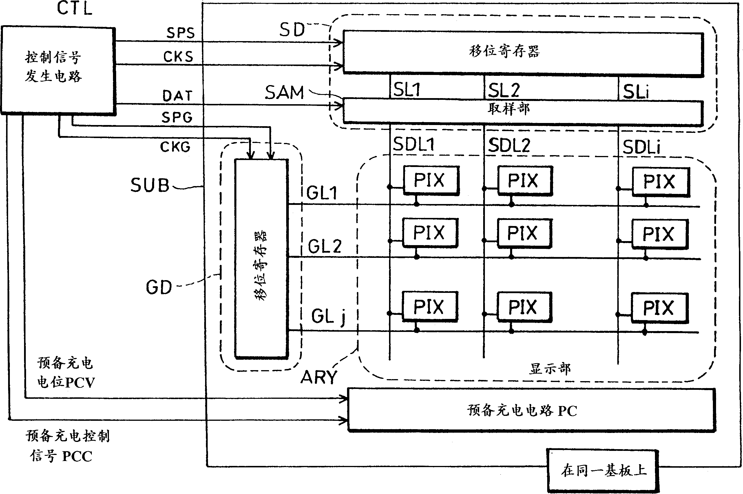
[0078] figure 2 It is a block diagram showing an example of the structure of the image display device of the present invention. This block diagram consists of a data signal line drive circuit SD, a scan signal line drive circuit GD, a data signal line SDLn (1≤n≤i), a scan signal line GLn (1≤n≤j), a pixel PIX, a control signal generation circuit CTL and Preliminary charging circuit PC constitutes. In addition, the structure of the pixel PIX section is as Figure 12 shown.

[0079] Among them, such as Figure 12 As shown, the pixel PIX is composed of a switching element SW, a liquid crystal capacitor CL, and a storage capacitor CS. One end of the capacitor constituting the pixel PIX is connected to the data signal line SDL via the switching element SW, and the other end is connected to a common electrode called a counter electrode COM to apply a counter potential VCOM. ...

Embodiment 2

[0105] Another embodiment of the present invention will be described below.

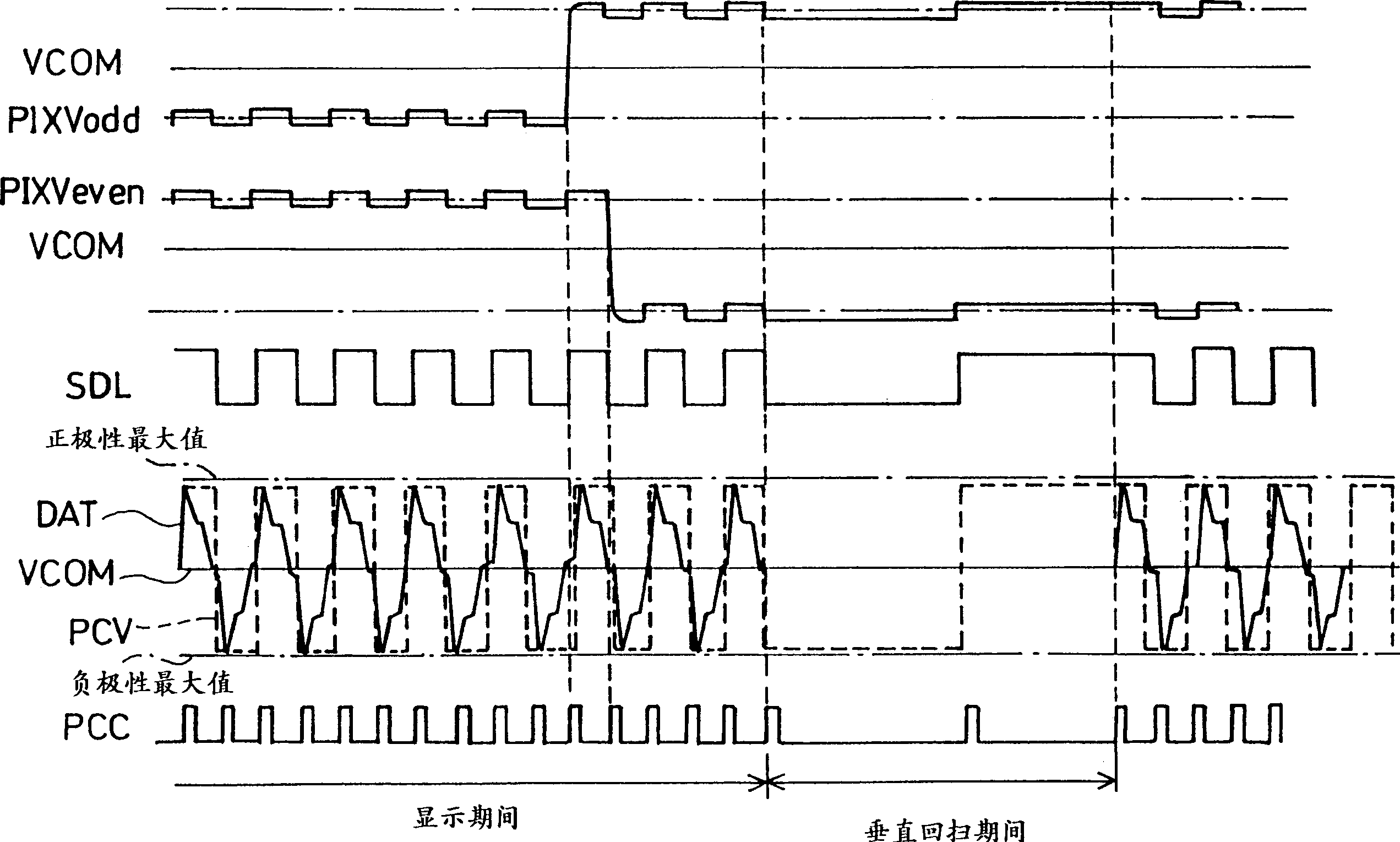
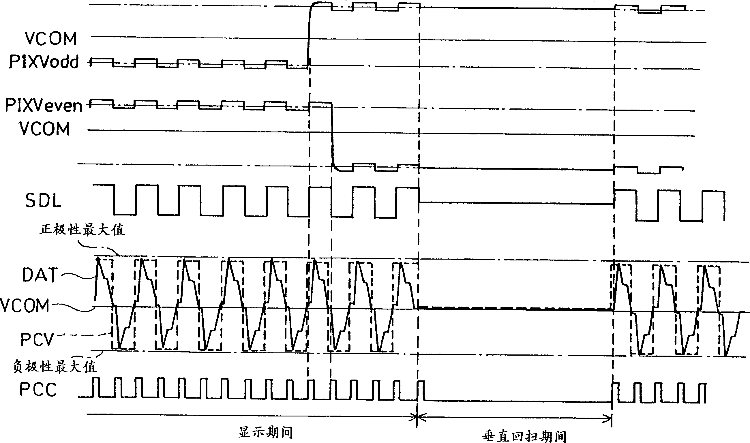
[0106] The liquid crystal display device of this embodiment has basically the same structure as that of Embodiment 1 above, except that the preliminary charge potential PCV has an AC potential synchronized with one line period (1H) of the image signal. The drive waveform of this example is shown in Figure 4 .

[0107] The driving waveform of this embodiment differs from the driving waveform used in the first embodiment only in the AC cycle of the pre-charging potential PCV and the timing of the pre-charging potential PCC, and the driving method and functions of each part are the same as those in the first embodiment.

[0108] As in the present embodiment, the method of constituting a signal of a fixed period synchronized with one line period (1H) for one signal has the advantage of being easier to manufacture than the case of constituting one signal with a plurality of periods.

[0109] Such as ...

Embodiment 3

[0117] Another embodiment of the present invention will be described below.

[0118] The liquid crystal display device of this embodiment has basically the same structure as that of Embodiment 1 described above.

[0119] The preliminary charge potential PCV in the vertical retrace period in this embodiment has an AC potential of not less than 50% of the maximum value of the image signal in positive polarity and not less than 50% of the maximum value in negative polarity. The driving waveforms of each part at this time are as follows Figure 5 shown.

[0120] Figure 5 The drive waveform shown is different from that of the second embodiment only in the pre-charge potential PCV during the vertical retrace period, and the driving method and functions of each part are the same as those of the second embodiment.

[0121] In this way, the potential can be selected according to the degree of fluctuation of the pixel potential, and the precharge potential PCV in the vertical retrac...


PUM

PropertyMeasurementUnit
strain pointaaaaaaaaaa

Abstract

In a vertical retrace interval, a pre-charge potential or a signal potential is applied to each polarity for AC driving liquid crystal at least once each, so as to maintain fluctuations in pixel potential between the positive polarity side and the negative polarity side uniform, and minimum required potentials are supplied to the data signal line, thereby suppressing decrease in image quality without significantly increasing power consumption.

Description

technical field [0001] The present invention relates to a driving method of an image display device, in particular to an image display device and a driving method thereof which control pixel potential fluctuations in liquid crystal AC driving of a liquid crystal display device and suppress pixel deterioration. Background technique [0002] Next, an active matrix type liquid crystal display device as an example of a conventional image display device will be described. Such as Figure 11 As shown, the active matrix liquid crystal display device is composed of a pixel array ARY, a scanning signal line driving circuit GD, a data signal line driving circuit SD and a pre-charging circuit PC. [0003] The above-mentioned pixel array ARY includes a plurality of scanning signal lines GL1 to GLj and data signal lines SDL1 to SDLj crossing each other. In addition, the pixels PIX are arranged in a matrix in each region surrounded by two adjacent scanning signal lines GL and two adjacen...

Claims


Application Information

Patent Timeline
Patent Type & Authority Patents(China)
IPC IPC(8): G02F1/133G09G3/20G09G3/36H04N5/66
CPCG09G3/3648G09G2310/0251G09G2320/0233G09G3/3614G09G3/36
Inventor 鹫尾一枽原信弘吉田茂人麻生祐史米田裕
Owner SHARP KK
Why Eureka
Try Eureka