Solid-state imaging device, manufacturing method of solid-state imaging device, and electronic device

A solid-state imaging device and pixel technology, which is applied in the direction of electric solid-state devices, radiation control devices, circuits, etc., can solve the problems of reduced focus detection accuracy, image quality degradation, and light reduction.

Active Publication Date: 2020-09-18
SONY CORP
View PDF6 Cites 0 Cited by
  • Summary
  • Abstract
  • Description
  • Claims
  • Application Information

AI Technical Summary

Problems solved by technology

[0006] However, when dichroic filters are formed in focus detection pixels, it may happen that the amount of light necessary for focus detection is reduced, resulting in a decrease in the accuracy of focus detection
In addition, when a half mirror member is provided in a focus detection pixel, it may occur that ghosting occurs due to irregular reflection of incident light, resulting in deterioration of image quality of an image.

Method used


Image

  • Solid-state imaging device, manufacturing method of solid-state imaging device, and electronic device
  • Solid-state imaging device, manufacturing method of solid-state imaging device, and electronic device
  • Solid-state imaging device, manufacturing method of solid-state imaging device, and electronic device

Examples


Embodiment Construction

[0028] Hereinafter, embodiments of the present technology will be described with reference to the drawings.

[0029] Construction example of a solid-state imaging device

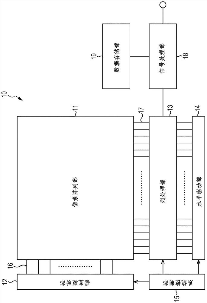
[0030] figure 1 is a block diagram showing an example of a solid-state imaging device to which the present technology is applied. The following description is directed to the structure of a surface-illuminated complementary metal oxide semiconductor (CMOS: Complementary Metal Oxide Semiconductor) image sensor, which is one of amplifying solid-state imaging devices. This technology can be applied not only to surface-illuminated CMOS image sensors, but also to back-illuminated CMOS image sensors or charge-transport solid-state imaging devices, such as other amplifying solid-state imaging devices and charge-coupled devices (CCDs). : ChargeCoupled Device) image sensor and the like.

[0031] figure 1 The illustrated CMOS image sensor 10 is configured to have: a pixel array section 11 formed on a semiconductor...


PUM

PropertyMeasurementUnit
thicknessaaaaaaaaaa
refractive indexaaaaaaaaaa

Abstract

There is provided a solid-state imaging device which includes a plurality of pixels including an imaging pixel for generating a captured image and a focus detection pixel for detecting a focus, in which the focus detection pixel includes a microlens, a photoelectric conversion unit which receives light incident from the microlens, a light-shielding unit which shields a portion of light incident on the photoelectric conversion unit, and a dimming filter which dims the light incident on the photoelectric conversion unit and is formed to contain a black pigment. The present technology can be applied to, for example, a CMOS image sensor.

Description

technical field [0001] The present technology relates to a solid-state imaging device, a method of manufacturing the solid-state imaging device, and electronic equipment, and more particularly, to a solid-state imaging device, a method of manufacturing the solid-state imaging device, and electronic equipment capable of maintaining the accuracy of focus detection and suppressing image quality degradation of images. Background technique [0002] As a method for detecting focus in a solid-state imaging device, a so-called split-pupil type phase-difference focus detection method has been used, in which focus detection pixels are generated in conjunction with a sensor passing through an optical system. A pair of image signals corresponding to the image formed by the light beams, and the focus is detected based on the amount of deviation of the pair of generated image signals. [0003] However, since the imaging pixels and the focus detection pixels provided in the pixel area have...

Claims


Application Information

Patent Timeline
Patent Type & Authority Patents(China)
IPC IPC(8): H01L27/146
CPCH01L27/14621H01L27/14623H01L27/14627H01L27/14685
Inventor 原沢正规关勇一狭山征博
Owner SONY CORP
Why Eureka
Try Eureka