
Bearing device, reaction chamber and semiconductor processing equipment

A technology of carrying device and reaction chamber, used in semiconductor/solid-state device manufacturing, electrical components, circuits, etc., can solve the failure of the robot to take or place the film, reduce the production efficiency, and the contact area between the robot and the workpiece to be processed cannot correspond, etc. problems, to achieve the effect of improving efficiency, improving accuracy, and improving economic benefits

Active Publication Date: 2015-09-09
BEIJING NAURA MICROELECTRONICS EQUIP CO LTD
View PDF3 Cites 2 Cited by
  • Summary
  • Abstract
  • Description
  • Claims
  • Application Information

AI Technical Summary

Problems solved by technology

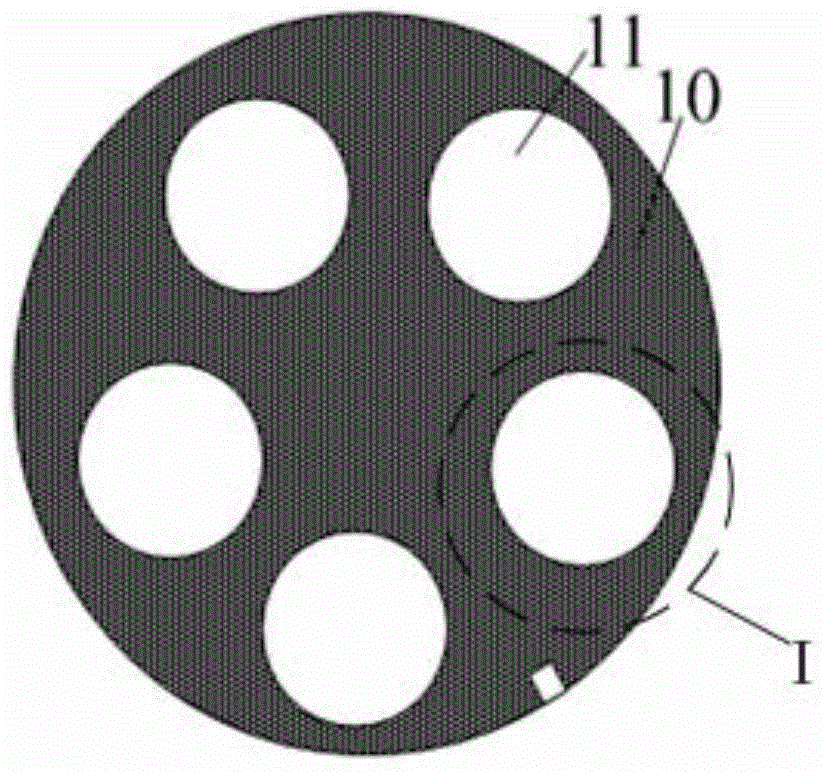
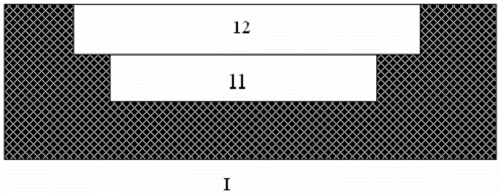
[0004] However, the above-mentioned tray inevitably has the following problems in practical applications: in order to reduce the pollution and damage of the processed workpiece caused by the adsorption contact between the manipulator and the processed workpiece, the contact area between the manipulator and the processed workpiece is usually minimized , and this will cause such a problem, that is, once there is a deviation in the levelness of the upper surface of the tray 101 relative to the manipulator, there will be a problem that the contact area between the manipulator and the processed workpiece cannot correspond, resulting in the failure of the manipulator to take or put the film , thereby reducing production efficiency

Method used


Image

  • Bearing device, reaction chamber and semiconductor processing equipment
  • Bearing device, reaction chamber and semiconductor processing equipment
  • Bearing device, reaction chamber and semiconductor processing equipment

Examples


Embodiment Construction

[0030] In order for those skilled in the art to better understand the technical solution of the present invention, the carrying device, reaction chamber and semiconductor processing equipment provided by the present invention will be described in detail below with reference to the accompanying drawings.

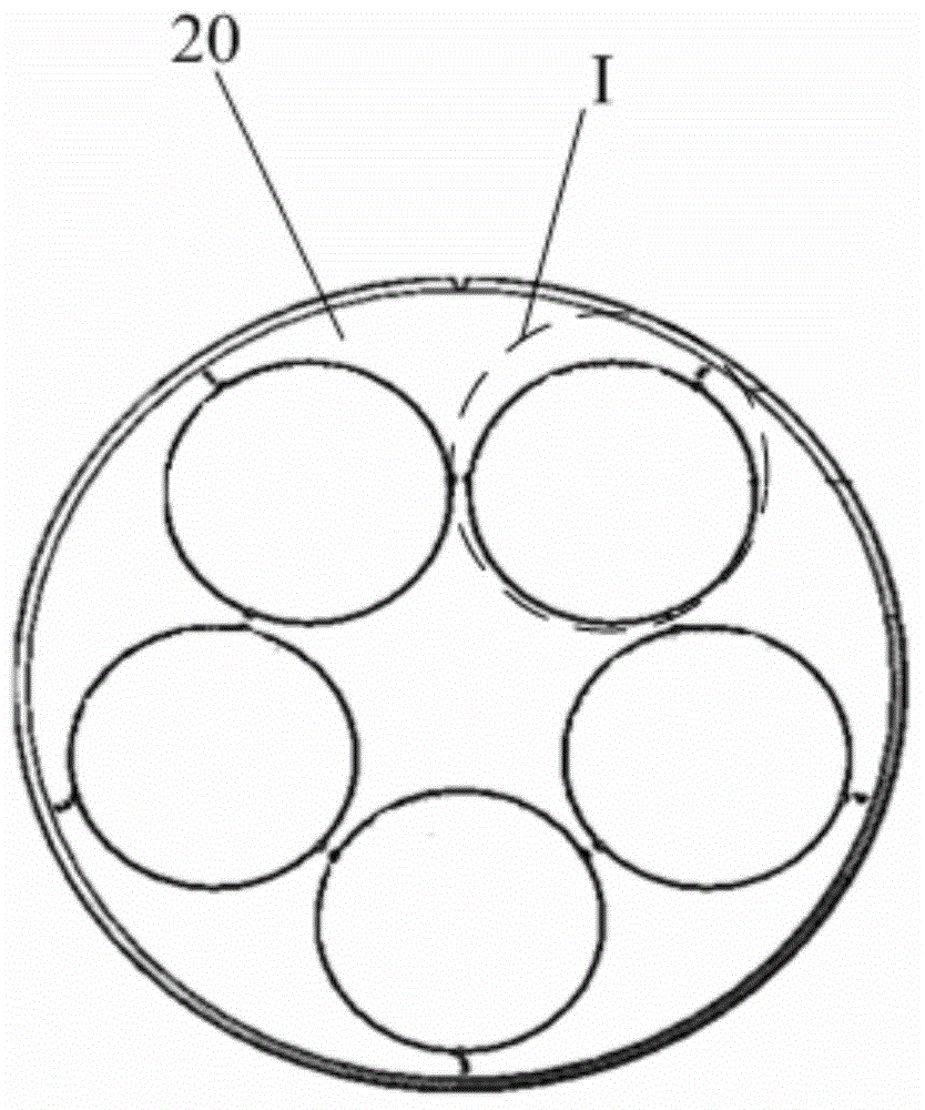
[0031] image 3 It is a top view of the tray of the carrying device provided by the present invention. Figure 4 for image 3 A first cross-sectional view of area I of the pallet shown. Figure 5 It is a schematic diagram of the structure of the auxiliary parts. Figure 6 for image 3 Top view of area I of the tray shown. Please also refer to image 3 , Figure 4 , Figure 5 with Figure 6 , the carrying device provided in this embodiment includes a tray 20 and auxiliary parts 21, wherein a plurality of first grooves 201 are arranged on the upper surface of the tray 20, and the workpiece S to be processed is placed in the first grooves 201, and each At least three se...


PUM


Abstract

The invention provides a bearing device, a reaction chamber and semiconductor processing equipment. The bearing device comprises a tray and auxiliary members. When a processed workpiece is not placed in first grooves, the first extension ends of the auxiliary members are higher than the bottom surfaces of the first grooves. In the process of placing the processed workpiece in the first grooves, the first extension ends are downwardly pressed by the gravity effect of the processed workpiece so that the first extension ends are enabled to rotate around the rotating shafts of the auxiliary members into second grooves and drive the second extension ends of the auxiliary members to rotate and rise around rotating shafts simultaneously. In the process that a manipulator acquires the processed workpiece in the first grooves, the second extension ends are downwardly pressed by the gravity effect of the manipulator so that the second extension ends are enabled to fall around the rotating shafts and drive the first extension ends to rotate and rise around the rotating shafts simultaneously, and thus the first extension ends are enabled to be jacked up by the processed workpiece. According to the bearing device, efficiency of processed workpiece absorption of the manipulator can be enhanced and accuracy of processed workpiece absorption of the manipulator can also be enhanced.

Description

technical field [0001] The invention belongs to the field of semiconductor equipment manufacturing, and in particular relates to a carrying device, a reaction chamber and semiconductor body processing equipment. Background technique [0002] In chemical vapor deposition (CVD) equipment, in order to increase the number of processed workpieces that can be processed in a single process and improve production efficiency, a tray that can carry multiple processed workpieces is usually set in the reaction chamber. And with the help of the manipulator, the pick-up or release of multiple workpieces to be processed is completed. [0003] figure 1 A top view of an existing pallet. figure 2 for figure 1 Sectional view of area I of the tray shown. Please also refer to figure 1 with figure 2 , the upper surface of the tray 10 is provided with a plurality of grooves spaced along its circumference, and each groove adopts a method such as figure 2 The stepped structure shown, that ...

Claims


Application Information

Patent Timeline
Patent Type & Authority Applications(China)
IPC IPC(8): H01L21/67H01L21/687
CPCH01L21/67011H01L21/68714
Inventor 李红
Owner BEIJING NAURA MICROELECTRONICS EQUIP CO LTD
Learn More