
Chip cleaning method and device

A chip cleaning and chip technology, applied in cleaning methods and utensils, cleaning methods using liquids, chemical instruments and methods, etc., can solve problems such as static electricity generated by chips, and achieve the effects of easy release and reduced water resistance.

Inactive Publication Date: 2015-09-23
SEMICON MFG INT (SHANGHAI) CORP +1
View PDF6 Cites 9 Cited by
  • Summary
  • Abstract
  • Description
  • Claims
  • Application Information

AI Technical Summary

Problems solved by technology

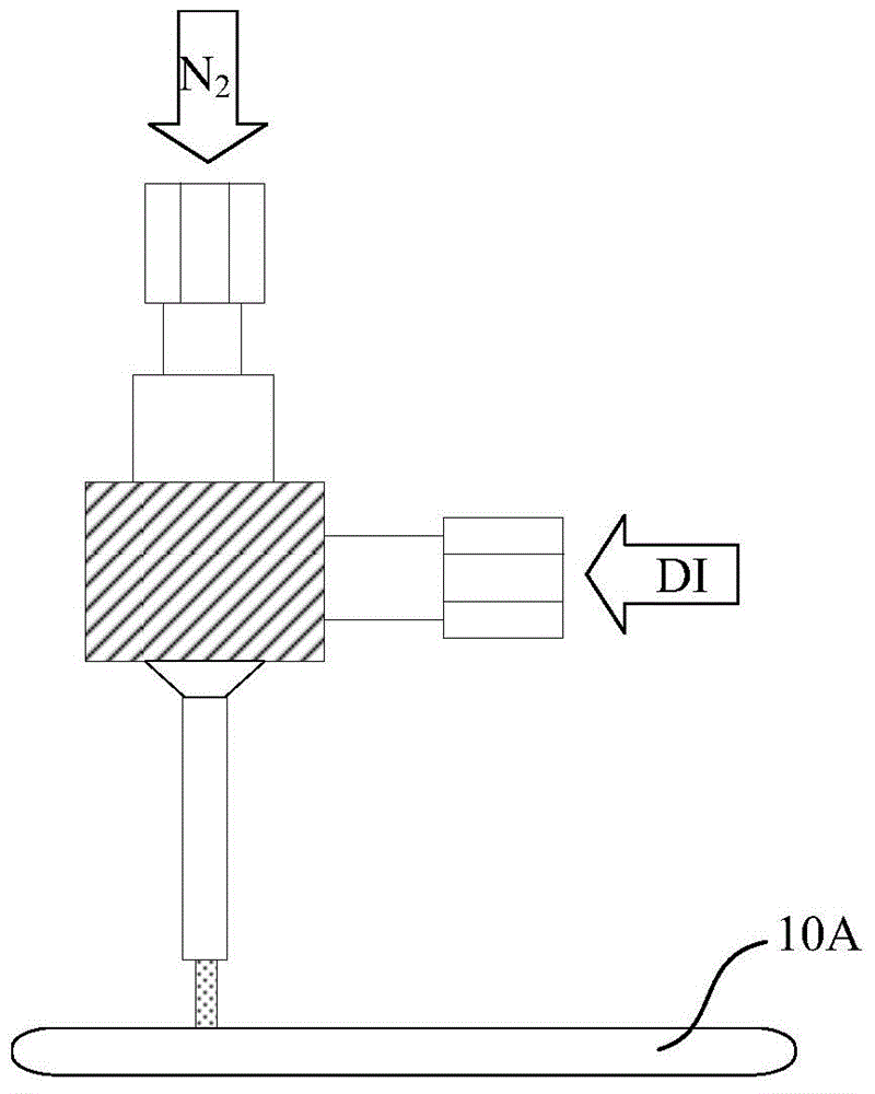
[0006] In view of the shortcomings of the prior art described above, the purpose of the present invention is to provide a chip cleaning method and device for solving the problem of static electricity generated inside the chip caused by atomization and spray cleaning in the prior art.

Method used


Image

  • Chip cleaning method and device
  • Chip cleaning method and device

Examples


Embodiment 1

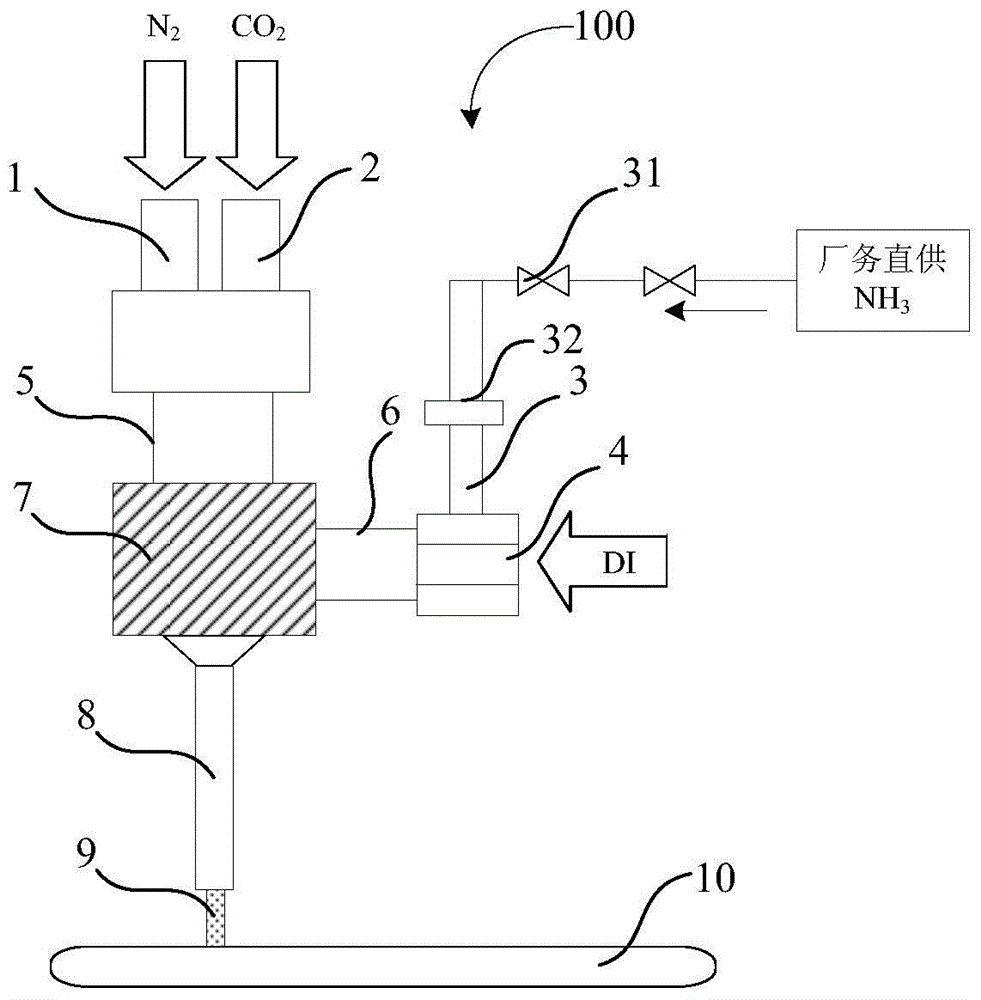
[0039] The invention provides a chip cleaning method. The chip cleaning method at least includes an atomization and spraying step. In the atomization and spraying step, a cleaning agent is sprayed on the chip surface to be cleaned by an atomization and spraying device; the cleaning agent includes A gas-liquid mixture of nitrogen, ammonia, carbon dioxide and deionized water (DI); the water resistance of the mixed liquid in the gas-liquid mixture is 50-80KΩ·CM. The atomization cleaning device such as figure 2 shown.

[0040] Specifically, the chip includes a semiconductor substrate and a device structure and a metal interconnection structure fabricated on the semiconductor substrate.

[0041] When using the chip cleaning method provided by the present invention, the cleaning agent comprising nitrogen, ammonia, carbon dioxide and deionized water is first passed into the atomization spray cleaning device 100 through each corresponding inlet, and then the cleaning agent is passed...

Embodiment 2

[0058] The present invention also provides a chip cleaning device, which is used in the chip cleaning method of Embodiment 1, such as figure 2 As shown, the chip cleaning device at least includes an atomization spray cleaning device 100, and the atomization spray cleaning device 100 includes a nitrogen gas introduction part 1, an ammonia gas introduction part 3, a carbon dioxide introduction part 2 and a deionized water introduction part 4, the The outlet of the nitrogen gas introduction part 1, the outlet 3 of the ammonia gas introduction part, the outlet of the carbon dioxide introduction part 2 and the outlet of the deionized water introduction part 4 communicate with a connecting piece 7, and the connecting piece 7 is also provided with a nozzle 8.

[0059] Further, the nitrogen introduction part 1 and the carbon dioxide introduction part 3 communicate with the connecting piece 7 through the first conduit 5, and the nitrogen and carbon dioxide introduced into the first con...


PUM


Abstract

The invention provides a chip cleaning method and device, and the method at least comprises an atomizing spraying and washing step. In the atomizing spraying and washing step, an atomizing spraying and washing device is used for enabling a cleaning agent to be sprayed on the surface of a chip to be cleaned. The cleaning agent is a gas-liquid mixture containing nitrogen, ammonia gas, carbon dioxide, and deionized water. The water resistance value of mixed liquid of the gas-liquid mixture is from 50 kilohm*cm to 80 kilohm*cm. According to the invention, the carbon dioxide and the ammonia gas are added into the cleaning agent, and are quickly acted in water, thereby generating a large number of positive negative ions: HCO3- and NH4+, enabling the water resistance value of the deionized water to be reduced, and enabling the static electricity of the surface of the chip to be discharged more easily.

Description

technical field [0001] The invention relates to the technical field of semiconductor manufacturing, in particular to a chip cleaning method and device. Background technique [0002] As the feature size of integrated circuits enters the deep sub-micron stage, the cleanliness of the chip surface required in the integrated circuit chip manufacturing process is getting higher and higher. In order to ensure the cleanliness of the chip material surface, digital Hundreds of cleaning processes, the cleaning process accounts for 30% of the entire manufacturing process. [0003] The traditional cleaning method is to use deionized water to rinse the chip. In this method, the deionized water hits the chip with a high flow rate to wash away the impurities and pollutants on the chip, so as to achieve the cleaning effect. However, this cleaning method has too much impact on the chip, which may easily cause damage to the element pattern, and the utilization rate of deionized water in this ...

Claims


Application Information

Patent Timeline
Patent Type & Authority Applications(China)
IPC IPC(8): B08B3/02H01L21/02H01L21/67
CPCB08B3/02H01L21/02057
Inventor 杨志勇杨勇
Owner SEMICON MFG INT (SHANGHAI) CORP
Learn More