Array substrate and liquid crystal display panel

An array substrate and black matrix technology, applied in the field of liquid crystal display, can solve problems such as corner light leakage, affecting display effect, and uneven pressing

Active Publication Date: 2015-09-23
XIAMEN TIANMA MICRO ELECTRONICS +1
View PDF8 Cites 14 Cited by
  • Summary
  • Abstract
  • Description
  • Claims
  • Application Information

AI Technical Summary

Problems solved by technology

[0004] The invention provides an array substrate and a liquid crystal display panel to solve the problems of uneven pressing and corner light leakage affecting the display effect

Method used


Image

  • Array substrate and liquid crystal display panel
  • Array substrate and liquid crystal display panel
  • Array substrate and liquid crystal display panel

Examples


Embodiment Construction

[0023] In order to make the purpose, technical solutions and advantages of the present invention clearer, the technical solutions of the present invention will be clearly and completely described through implementation with reference to the accompanying drawings of the embodiments of the present invention. Obviously, the described embodiments are part of the present invention Examples, not all examples. Based on the embodiments of the present invention, all other embodiments obtained by persons of ordinary skill in the art without making creative efforts belong to the protection scope of the present invention.

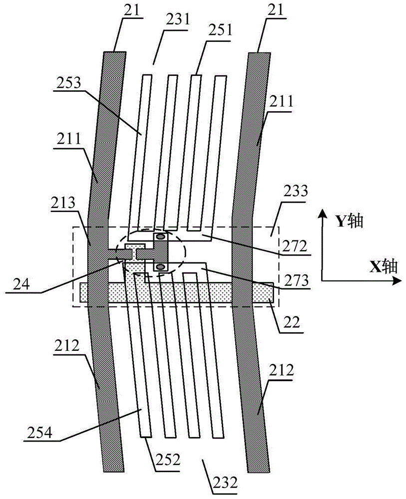
[0024] refer to Figure 2A As shown, it is a schematic structural diagram of the first array substrate provided by the embodiment of the present invention, and reference Figure 2B As shown in , it is a schematic structural diagram of a pixel region provided by an embodiment of the present invention. Wherein, the array substrate includes data lines 21 and scan lines ...


PUM


Abstract

The invention provides an array substrate, comprising data lines and scanning lines intersecting with each other, and a plurality of pixel regions. Each pixel region comprises a first photic region, a second photic region, and a shading region between the first photic region and the second photic region. The shading region is provided with a thin film transistor. The first photic region is provided with a first electrode. The second photic region is provided with a second electrode. The first electrode and the second electrode are respectively electrically connected with the drain electrode of the thin film transistor. The data line corresponding to each pixel region comprises a first part and a second part respectively extending to two directions. The first part and the second part are connected through a first connection portion which is in the shading region. The above technical scheme can solve a problem that uneven pressing influences display effect.

Description

technical field [0001] The invention relates to the technical field of liquid crystal display, in particular to an array substrate and a liquid crystal display panel. Background technique [0002] In the field of liquid crystal display technology, in-plane switching (In-Plane Switching IPS) technology and fringe field switching (Fringe Field Switching FFS) technology are two commonly used wide viewing angle liquid crystal display technologies. With the same substrate, the liquid crystal molecules are rotated in a plane parallel to the substrate, thereby improving the light transmission efficiency of the liquid crystal layer. [0003] At present, dual domain technology is widely used in IPS technology and FFS technology, figure 1 It is a schematic diagram of the pixel electrode structure using dual domain technology in the prior art, such as figure 1 As shown, data lines 11 and scan lines 12 are formed on the array substrate, and a plurality of pixel regions 13 are defined ...

Claims


Application Information

Patent Timeline
Patent Type & Authority Applications(China)
IPC IPC(8): G02F1/1362G02F1/1368G02F1/1343H01L27/12
CPCG02F1/134309G02F1/136209G02F1/136227G02F1/136286G02F1/1368H01L27/1214G02F1/134345G02F1/134372G02F1/133514H01L27/124
Inventor 吴昊宋琼
Owner XIAMEN TIANMA MICRO ELECTRONICS
Why Eureka
Try Eureka