Display base plate and manufacturing method of display base plate as well as display device

A display substrate and substrate substrate technology, which is applied in optics, instruments, electrical digital data processing, etc., can solve the problems of low light transmittance, thick module, high production cost of external touch screen, etc., to improve signal-to-noise Ratio, the effect of improving touch sensitivity and accuracy

Inactive Publication Date: 2016-06-01
BOE TECH GRP CO LTD +1
View PDF2 Cites 8 Cited by
  • Summary
  • Abstract
  • Description
  • Claims
  • Application Information

AI Technical Summary

Problems solved by technology

The production cost of the plug-in touch screen is high, the light transmittance is low, and the module is thick

Method used


Image

  • Display base plate and manufacturing method of display base plate as well as display device
  • Display base plate and manufacturing method of display base plate as well as display device
  • Display base plate and manufacturing method of display base plate as well as display device

Examples


Embodiment Construction

[0037] In order to enable those skilled in the art to better understand the technical solution of the present invention, the structure and principle of the present invention will be described in detail below in conjunction with the accompanying drawings. The examples given are only used to explain the present invention, not to limit the scope of protection of the present invention. .

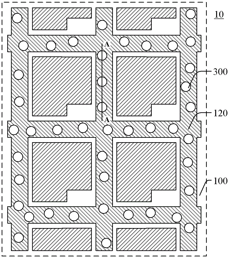
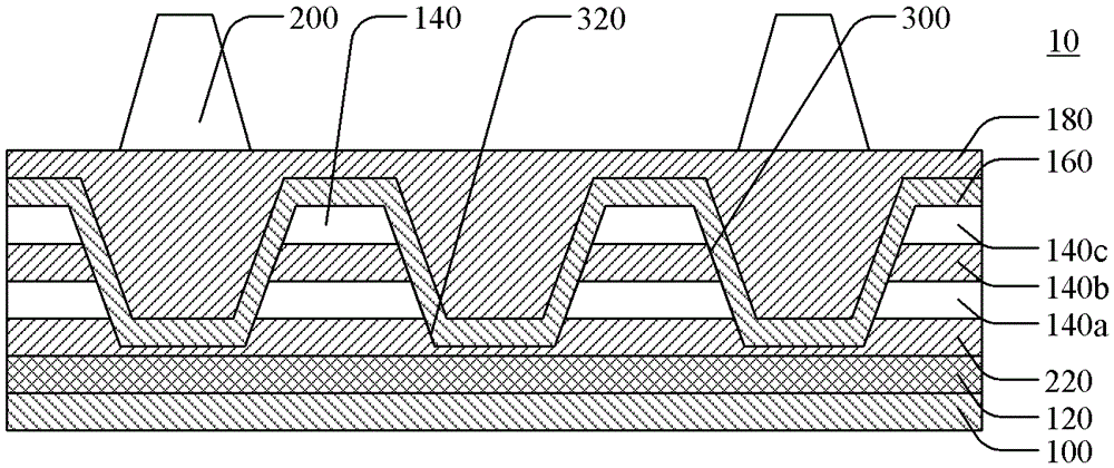
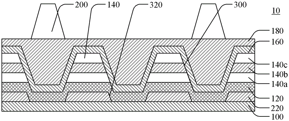
[0038] The components shown in the drawings are marked as follows: 10 display substrate; 100 base substrate; 120 black matrix; 140 filter layer stack; 140a, 140b, 140c color filter layer; 160 touch electrode; 200 a spacer; 220 a first protective layer; 300 an opening; 310 a first depression; 320 a second depression; 330 a third depression.

[0039] figure 1 It is a schematic top view of a part of a display substrate according to an embodiment of the present invention. Figure 2A , 2B , 2C, 2D and 2E are respectively along figure 1 Schematic cross-sectional view of line A-A. As shown, the di...


PUM


Abstract

The invention discloses a display base plate and a manufacturing method of the display base plate as well as a display device. The display base plate comprises a substrate base plate, a patterned black matrix and a touch electrode, wherein the patterned black matrix is arranged on the substrate base plate; in the region of the black matrix, the display base plate comprises a light filtering layer laminating layer located on the black matrix; the light filtering layer laminating layer comprises more than two colored light filtering layers which are stacked in sequence, and is provided with a plurality of openings; the touch electrode is arranged on the light filtering layer laminating layer and covers the surface provided with the plurality of openings. According to the display base plate disclosed by the invention, the light filtering layer laminating layer provided with the plurality of openings is arranged in the region of the black matrix of the display base plate, so that the surface area of the touch electrode, covered by the light filtering layer laminating layer, is enlarged, and more charges can be easily gathered, and furthermore, the touch sensitivity and the touch accuracy are improved.

Description

technical field [0001] The present invention relates to the field of display technology, and in particular to a display substrate, a manufacturing method thereof, and a display device. Background technique [0002] At present, smart devices generally adopt touch technology to realize human-computer interaction. Touch panels (touch panels) can be classified into add-on touch panels, on-cell touch panels and in-cell touch panels according to their composition and structure. The plug-in touch screen is produced separately from the touch screen and the LCD panel, and then bonded to the LCD panel to have a touch function. The production cost of the plug-in touch screen is high, the light transmittance is low, and the module is thick. In the surface-covered touch screen, the touch electrodes are arranged between the color filter substrate and the polarizer of the liquid crystal panel. In the embedded touch screen, the touch electrodes are arranged inside the liquid crystal pane...

Claims


Application Information

Patent Timeline
Patent Type & Authority Applications(China)
IPC IPC(8): G02F1/1333G02F1/1335G02F1/1343G06F3/044
CPCG02F1/13338G02F1/133512G02F1/133514G02F1/134309G06F3/044G02F1/133516G06F3/0412G06F2203/04103G06F3/0443G02F1/136222G02F1/133519G02F1/13394
Inventor 王亮
Owner BOE TECH GRP CO LTD
Why Eureka
Try Eureka