Thin film transistor device and preparation method therefor

A thin-film transistor and device technology, applied in the field of thin-film transistor devices and their preparation, can solve the problem of large off-state current, achieve the effects of reducing off-state current, simple process, and improving performance

Inactive Publication Date: 2016-07-20
KUNSHAN GO VISIONOX OPTO ELECTRONICS CO LTD
View PDF2 Cites 10 Cited by
  • Summary
  • Abstract
  • Description
  • Claims
  • Application Information

AI Technical Summary

Problems solved by technology

[0006] The purpose of the present invention is to provide a thin film transistor device and its preparation method, which solves the problem of large off-state current of the thin film transistor device, improves the electrical performance and uniformity of the device, and does not increase the difficulty of the process

Method used


Image

  • Thin film transistor device and preparation method therefor
  • Thin film transistor device and preparation method therefor
  • Thin film transistor device and preparation method therefor

Examples


Embodiment 1

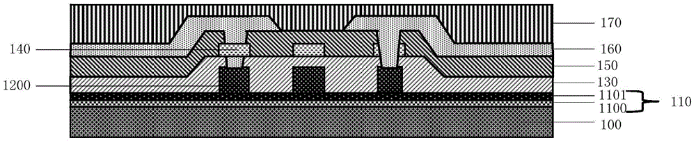
[0027] Please refer to figure 1 , which is a schematic cross-sectional view of the thin film transistor device provided in Embodiment 1 of the present invention. Such as figure 1 As shown, the thin film transistor device sequentially includes: a substrate 100, a buffer layer 110, a channel layer 120, a gate insulating layer 130, a gate 140, an interlayer insulating layer 150, and a source and drain 160; the channel layer 120 is curved in shape.

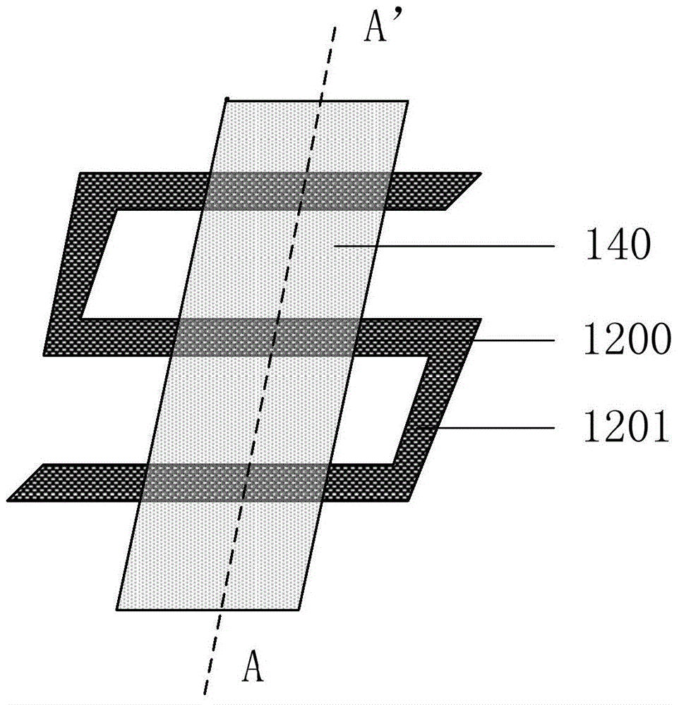
[0028] Please refer to figure 2 , which is a schematic structural view of the channel layer in the thin film transistor device provided in Embodiment 1 of the present invention, as shown in figure 2 As shown, in this embodiment, the shape of the channel layer 120 is S-type, and the channel layer 120 includes a channel layer 1200 in an undoped region and a channel layer 1201 in a doped region. The projection of the channel layer 1200 on the substrate 100 is located in the projection area of ​​the gate 140 on the substrate 100, th...

Embodiment 2

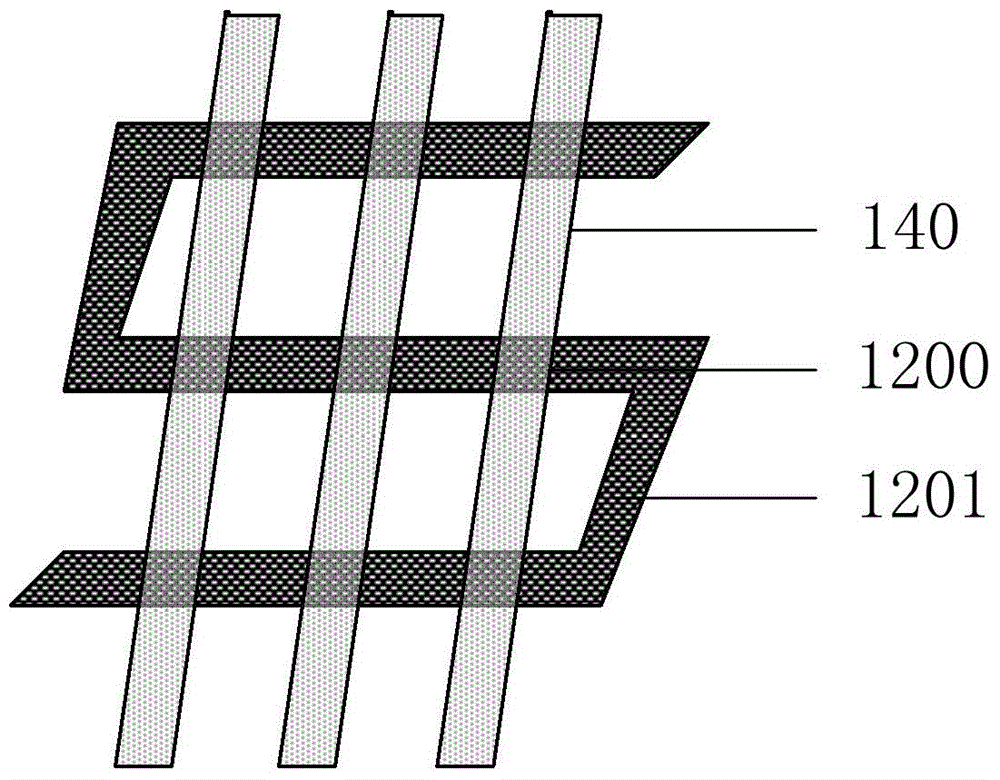
[0039] On the basis of Embodiment 1, the thin film transistor device is a multi-gate S-channel, such as image 3 As shown, since its cross-sectional view and preparation method are consistent with Embodiment 1, it is not repeated here.

[0040] The multi-gate S-channel can adjust the length and width of the thin film transistor device, so as to obtain a thin film transistor device with better matching process and design.

[0041] To sum up, the thin film transistor device and its preparation method provided by the present invention, by setting the channel layer of the thin film transistor device in a curved shape, avoids the impact on the device pixels due to the length of the channel being too long, and the channel layer The length and width can be adjusted according to the needs, which solves the problem that the channel layer is long in one direction; the present invention arranges the channel layer in the non-doped region in the area covered by the gate, and the channel la...


PUM


Abstract

The invention provides a thin film transistor device and a preparation method therefor. The thin film transistor device comprises a substrate, a buffer layer, a channel layer, a gate insulating layer, gate electrodes, an interlayer insulating layer, and a source electrode and a drain electrode in sequence, wherein the channel layer is bent, so that influence on the pixel of the device from the overlong length of the channel can be avoided; the length and the width of the channel layer can be both adjusted according to needs, so that the problem of relatively long channel layer in a single direction is well solved; in addition, the channel region in a non-doping region is arranged in a region which is covered with the gate electrodes; the channel layer in a doping region is arranged outside the region which is covered with the gate electrodes, so that a PN junction is formed in the contact interface between the channel layer in the non-doping region and the channel layer in the doping region; therefore, the off-state current of the thin film transistor device is lowered consequently; the performance of the device is improved to a large extent; and meanwhile, the device instability caused by an electric field effect between the source electrode and the drain electrode can be well avoided.

Description

technical field [0001] The invention relates to the technical field of semiconductors, in particular to a thin film transistor device and a preparation method thereof. Background technique [0002] Active matrix Organic Light-Emitting Diode (AMOLED) display technology that combines thin film transistor (ThinFilmTransistor, TFT) devices with Organic Light-Emitting Diode (OLED) technology is an important development direction for current and future flat panel displays. When facing this kind of application, the reliability of TFT device is the device performance that the industry generally pays attention to. [0003] AMOLED usually uses low-temperature polysilicon as the active layer of the TFT backplane, so that the TFT device has a larger driving current, which is beneficial to the luminous brightness of the OLED. If a low-temperature polysilicon semiconductor is used as the channel layer, the grain boundary will greatly deteriorate the electrical performance of the TFT devi...

Claims


Application Information

Patent Timeline
Patent Type & Authority Applications(China)
IPC IPC(8): H01L29/786H01L21/336
Inventor 赵加湘
Owner KUNSHAN GO VISIONOX OPTO ELECTRONICS CO LTD
Why Eureka
Try Eureka