Thin film transistor, production method thereof, array substrate and display device

A technology of thin film transistors and manufacturing methods, which is applied in the direction of transistors, semiconductor/solid-state device manufacturing, electric solid-state devices, etc., can solve problems such as poor display contrast, influence of aperture ratio of display devices, large off-state current, etc., to improve display contrast, Improve the display effect and reduce the effect of off-state current

Inactive Publication Date: 2017-01-04
BOE TECH GRP CO LTD
View PDF4 Cites 10 Cited by
  • Summary
  • Abstract
  • Description
  • Claims
  • Application Information

AI Technical Summary

Problems solved by technology

[0004] At present, the arrayed CNT-TFT is prepared by solution coating process, and the active layer area forms carbon nanotubes with random network distribution. For short-channel TFTs, the off-state current is relatively large, about 10 -11 -10 -10 A. The off-state brightness of the TFT-LCD prepared on the basis of this performance is high, so the display contrast is also poor; and the use of long-channel TFTs can reduce the off-state current and increase the switching ratio, but the overall display device Aperture ratio can be greatly affected

Method used


Image

  • Thin film transistor, production method thereof, array substrate and display device
  • Thin film transistor, production method thereof, array substrate and display device
  • Thin film transistor, production method thereof, array substrate and display device

Examples


Embodiment 1

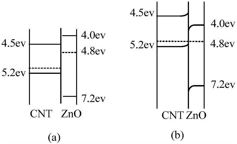
[0052] This embodiment provides a thin film transistor, the thin film transistor includes a gate, a gate insulating layer, a source, a drain and an active layer on a base substrate, between the active layer and the drain A unidirectional conduction device is formed, so that electrical signals are transmitted from the active layer to the drain via the unidirectional conduction device.

[0053] In this embodiment, a unidirectional conduction device is formed between the active layer and the drain of the thin film transistor. When the potential of the active layer is higher than the potential of the drain, the unidirectional conduction device is turned on; When the potential is lower than the potential of the drain, the unidirectional conduction device is cut off, thereby effectively reducing the off-state current of the thin film transistor. When the thin film transistor of the present invention is applied to a display device, the display contrast of the display device can be imp...

Embodiment 2

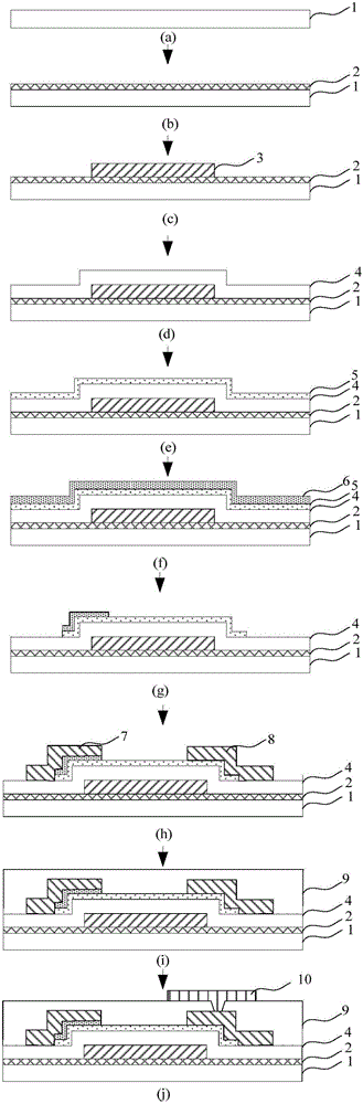
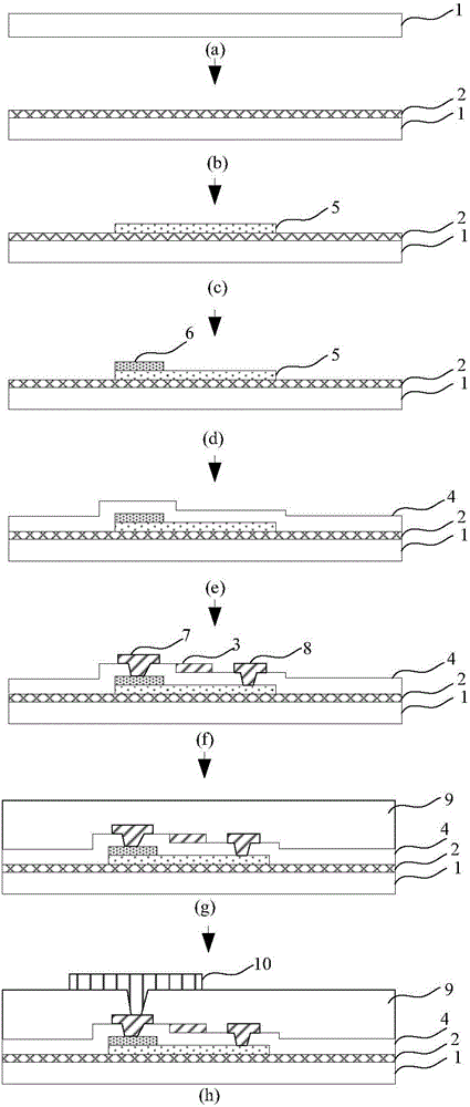
[0072] This embodiment provides a method for manufacturing a thin film transistor, including forming a gate, a gate insulating layer, a source, a drain, and an active layer on a substrate, and the method further includes:

[0073] A unidirectional conduction device is formed between the active layer and the drain, so that electrical signals are transmitted from the active layer to the drain through the unidirectional conduction device.

[0074] In this embodiment, a unidirectional conduction device is formed between the active layer and the drain of the thin film transistor. When the potential of the active layer is higher than the potential of the drain, the unidirectional conduction device is turned on; When the potential is lower than the potential of the drain, the unidirectional conduction device is cut off, thereby effectively reducing the off-state current of the thin film transistor. When the thin film transistor of the present invention is applied to a display device, ...

Embodiment 3

[0091] This embodiment provides an array substrate, including the thin film transistor mentioned above.


PUM


Abstract

The invention provides a thin film transistor, a production method thereof, an array substrate and a display device, and belongs to the technical field of display. The thin film transistor comprises a grid, a grid insulating layer, a source, a drain and an active layer which are positioned on a substrate; a one-way conducting device is arranged between the active layer and the drain, so that an electric signal is transmitted from the active layer to the drain through the one-way conducting device. According to the technical scheme of the invention, the off-state current of the thin film transistor can be effectively reduced, and the display effect of the display device can be improved.

Description

technical field [0001] The present invention relates to the field of display technology, in particular to a thin film transistor, a manufacturing method thereof, an array substrate and a display device. Background technique [0002] The demand for various display devices has increased with the rise of the global information society. Therefore, much effort has been devoted to the research and development of various flat display devices, such as liquid crystal displays (LCDs), plasma display panels (PDPs), electroluminescent displays (ELDs), and vacuum fluorescent displays (VFDs). [0003] Thin Film Transistor (TFT) is a key electronic device in modern microelectronics technology, and has been widely used in flat panel displays and other fields. Thin film transistors in the traditional semiconductor industry and TFT-LCD display industry are based on silicon materials, and carbon-based semiconductor materials are a new generation of semiconductor materials because of their hig...

Claims


Application Information

Patent Timeline
Patent Type & Authority Applications(China)
IPC IPC(8): H01L27/12H01L29/786H01L21/336
CPCH01L29/78639H01L27/1214H01L27/1259
Inventor 李延钊孟虎毛德丰
Owner BOE TECH GRP CO LTD
Why Eureka
Try Eureka