Thin film transistor liquid crystal display (TFT-LCD) array substrate and manufacturing method thereof

An array substrate and substrate technology, applied in semiconductor/solid-state device manufacturing, instruments, semiconductor devices, etc., can solve the problems of excessive TFT off-state current, shortened pixel electrode charge retention time, and affecting TFT performance, etc., to reduce The effects of off-state current, prolonging the charge retention time of the pixel electrode, and improving TFT performance

Active Publication Date: 2010-07-07
K TRONICS (SUZHOU) TECH CO LTD +1
View PDF0 Cites 10 Cited by
  • Summary
  • Abstract
  • Description
  • Claims
  • Application Information

AI Technical Summary

Problems solved by technology

[0006] The purpose of the present invention is to provide a TFT-LCD array substrate and a manufacturing method thereof, which overcomes the excessive off-state current of the TFT caused by the thicker semiconductor layer in the four-time patterning process of the prior art, and the shortening of the charge retention time of the pixel electrodes. Defects in TFT performance

Method used


Image

  • Thin film transistor liquid crystal display (TFT-LCD) array substrate and manufacturing method thereof
  • Thin film transistor liquid crystal display (TFT-LCD) array substrate and manufacturing method thereof
  • Thin film transistor liquid crystal display (TFT-LCD) array substrate and manufacturing method thereof

Examples


no. 1 example

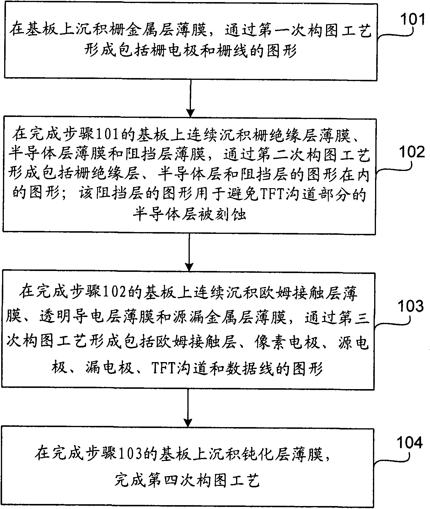
[0041] Such as figure 2 The flow chart of the first embodiment of the manufacturing method of the TFT-LCD array substrate of the present invention is shown, including:

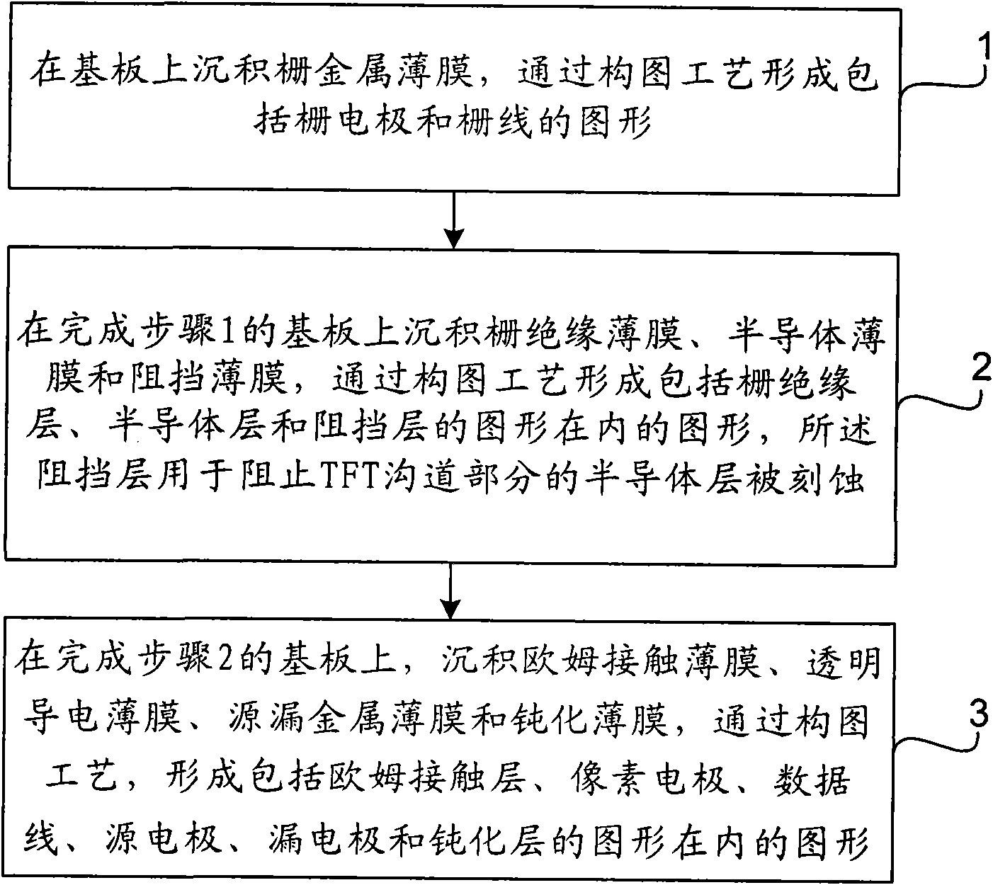
[0042] Step 101: Deposit a gate metal layer film on a substrate, and form a pattern including gate electrodes and gate lines through a first patterning process;

[0043] Step 102: successively deposit a gate insulating layer film, a semiconductor layer film, and a barrier layer film on the substrate after step 101, and form patterns including patterns of the gate insulating layer, the semiconductor layer and the barrier layer through the second patterning process; The pattern of the barrier layer is used to prevent the semiconductor layer of the TFT channel part from being etched;

[0044] Step 103: Continuously deposit an ohmic contact layer film, a transparent conductive layer film, and a source-drain metal layer film on the substrate after step 102, and form an ohmic contact layer, pixel electrode, source electro...

no. 2 example

[0058] Such as Figure 7 Shown is a flowchart of a second embodiment of a method for manufacturing a TFT-LCD array substrate of the present invention, and the method includes:

[0059] Step 201: Deposit a gate metal layer film on a substrate, and form a pattern including gate electrodes and gate lines through the first patterning process;

[0060] Step 202: successively deposit a gate insulating layer film, a semiconductor layer film, and a barrier layer film on the substrate after step 201, and form patterns including patterns of the gate insulating layer, the semiconductor layer, and the barrier layer through the second patterning process; The pattern of the barrier layer is used to prevent the semiconductor layer of the TFT channel part from being etched;

[0061] Step 203: Continuously deposit an ohmic contact layer film, a transparent conductive layer film, and a source / drain metal layer film on the substrate after step 202, and form an ohmic contact layer, a pixel electrode, a ...


PUM

PropertyMeasurementUnit
thicknessaaaaaaaaaa
thicknessaaaaaaaaaa

Abstract

The invention relates to a thin film transistor liquid crystal display (TFT-LCD) array substrate and a manufacturing method thereof, wherein the manufacturing method comprises the following steps of: 1, depositing a gate metal-layer thin film on a substrate, forming a figure comprising a gate electrode and a gate line; 2, depositing a gate insulating layer thin film, a semiconductor layer thin film and a barrier layer thin film on the on the substrate subjected to the step 1, forming a figure comprising figures of a gate insulating layer, a semiconductor layer and a barrier layer, wherein the barrier layer is used for preventing the semiconductor layer of a thin film transistor (TFT) channel from being etched; and 3, depositing an ohmic contact layer thin film, a transparent conductive layer thin film, a source-drain metal layer thin film and a passivation layer thin film on the substrate subjected to the step 2, and forming a figure comprising figures of an ohmic contact layer, a pixel electrode, a data line, a source electrode, a drain electrode and a passivation layer. The invention can reduce the thickness of the semiconductor layer under the condition without increasing composition processes and enhance the performance of a thin film transistor (TFT) by arranging the barrier layer between the semiconductor layer and the ohmic contact layer in a clamping way.

Description

Technical field [0001] The invention relates to a method for manufacturing a thin film transistor liquid crystal display, in particular to a thin film transistor liquid crystal display (TFT-LCD) array substrate and a method for manufacturing the same. Background technique [0002] TFT-LCD has the characteristics of small size, low power consumption, and no radiation, and it occupies a dominant position in the current flat panel display market. For TFT-LCD, the array substrate structure and manufacturing process determine its product performance, yield and price. [0003] In order to effectively reduce the price of TFT-LCD and increase the yield rate, the manufacturing process of the TFT-LCD array substrate structure (active drive TFT array) has been gradually simplified. From the beginning, the 7mask process has been developed to the current Four patterning (4mask) process of slit lithography technology. [0004] In the prior art, the four patterning process uses a gray tone or hal...

Claims


Application Information

Patent Timeline
Patent Type & Authority Applications(China)
IPC IPC(8): G02F1/1362H01L27/12H01L21/84
CPCH01L29/78696H01L27/1214H01L27/12H01L29/78618H01L27/1288G02F1/1368H01L29/458H01L29/78606
Inventor 刘翔林承武陈旭谢振宇
Owner K TRONICS (SUZHOU) TECH CO LTD
Why Eureka
Try Eureka