Independent grid-controlled nano line field effect transistor

A technology of field effect transistors and nanowires, applied in semiconductor devices, electrical components, circuits, etc., to achieve the effect of reducing off-state current, reducing driving current, and strong driving ability

Active Publication Date: 2011-01-12
SEMICONDUCTOR MANUFACTURING INTERNATIONAL (BEIJING) CORP +1
View PDF0 Cites 10 Cited by
  • Summary
  • Abstract
  • Description
  • Claims
  • Application Information

AI Technical Summary

Problems solved by technology

Due to the limitation of short channel effect and gate leakage current, the traditional plana

Method used


Image

  • Independent grid-controlled nano line field effect transistor
  • Independent grid-controlled nano line field effect transistor
  • Independent grid-controlled nano line field effect transistor

Examples


Example Embodiment

[0023] 3) Complete the preparation of the outer gate structure; large-angle injection of phosphorus (1x10 15 cm -2 / 10keV) and annealing (1000℃ / 10s) to prepare source and drain regions;

[0024] 4) Standard CMOS process completes metal electrode preparation.

Example Embodiment

[0026] Embodiment 1. Independent gate controlled nanowire field effect transistor and its performance test

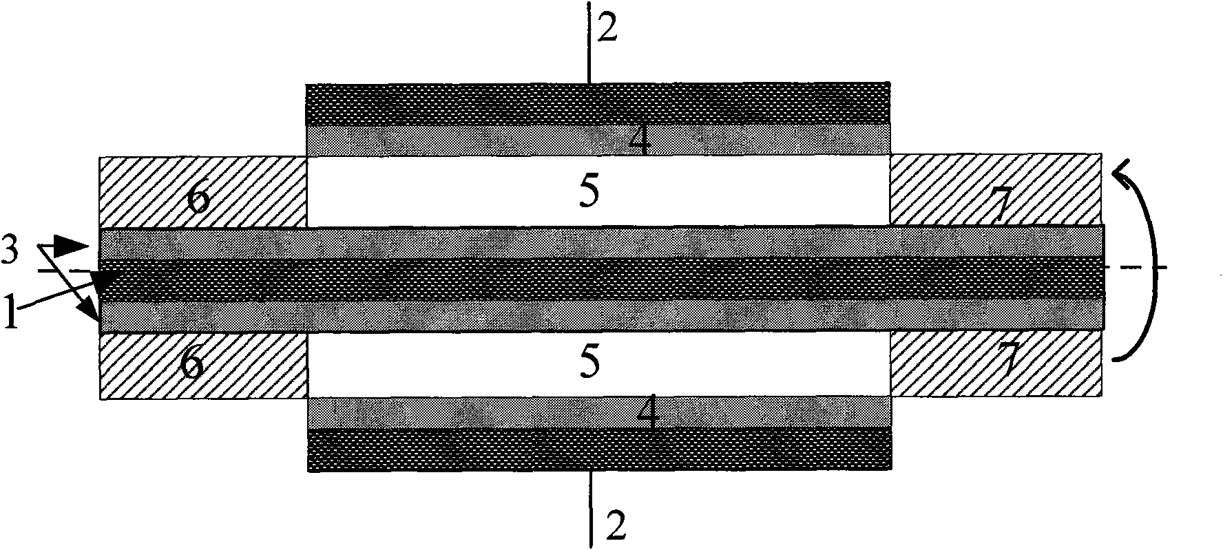
[0027] The structure of the independent gate controlled nanowire field effect transistor is as figure 1 As shown, the work function of the materials of the inner gate electrode 1 and the outer gate electrode 2 is set to 4.61 eV; the inner gate dielectric 3 and the outer gate dielectric 4 are silicon oxide layers with a thickness of 1.5 nm, and the channel region 5 is doped with boron Concentration 1×10 11 cm -3 Silicon material with a thickness of 10 nanometers; source region 6 and drain region 7 are doped with phosphorus with a concentration of 1×10 20 cm -3 The silicon material; the inner gate radius is 10 nanometers. The length of the source region and the drain region of the device are both 50 nanometers. The thickness of the source and drain regions is equal to the thickness of the channel region and surrounds the inner gate electrode.

[0028] The individual gate cont...


PUM

PropertyMeasurementUnit
Diameteraaaaaaaaaa
Thicknessaaaaaaaaaa
Thicknessaaaaaaaaaa

Abstract

The invention discloses an independent grid-controlled nano line field effect transistor which comprises an inner grid electrode, an outer grid electrode, inner and outer grid dielectric layers, a channel region, a source region and a drain region, wherein the inner grid electrode is positioned at the center of the whole device structure; and the inner grid dielectric, the channel region, the outer dielectric and the outer grid electrode are coaxially arranged from inside to outside to completely enclose the inner-layer region. The arrangement of the inner grid electrode can enable the nano line device to work under the condition of independent grid control so as to provide a selection scheme for the design of a low power consumption circuit, and the threshold voltage is more sensitive to the adjustment of the controlled electrode. When the device works under the common grid condition, the electrical performance of the device is superior to that of the conventional nano circular grid device and double grid device. For a silicon film thickness of 10nm, the independent grid-controlled nano line transistor device can shorten the grid length to 20nm.

Description

technical field [0001] The invention relates to a device for semiconductor integrated circuits, in particular to a nanowire field effect transistor controlled by an independent gate. Background technique [0002] The semiconductor industry has been developing rapidly in accordance with Moore's Law, and the size of transistors used in integrated circuits has been continuously reduced. Constrained by the short-channel effect and gate leakage current, the traditional planar bulk silicon technology will encounter the theoretical limit below the 32nm technology node. Devices with new structures continue to emerge, including silicon-on-insulator, double-gate, triple-gate, ring-gate and many other non-planar process devices. Among them, the gate-all-around device can provide excellent characteristics such as the strongest gate control capability, the smallest short-channel effect, and high switching current ratio due to the fully surrounded structure of the gate. It is considered ...

Claims


Application Information

Patent Timeline
IPC IPC(8): H01L29/78H01L29/423
Inventor 张立宁何进张健
Owner SEMICONDUCTOR MANUFACTURING INTERNATIONAL (BEIJING) CORP
Why Eureka
Try Eureka