Organic electroluminescent device and production method thereof

An electroluminescent device and electroluminescent layer technology, applied in the direction of circuits, electrical components, electric solid devices, etc., can solve the problems of large driving current, restricting the application of organic electroluminescent diodes, and low device life

Active Publication Date: 2013-06-05
OCEANS KING LIGHTING SCI&TECH CO LTD +1
View PDF3 Cites 10 Cited by
  • Summary
  • Abstract
  • Description
  • Claims
  • Application Information

AI Technical Summary

Problems solved by technology

[0004] Existing organic electroluminescent devices have large driving current, low luminous efficiency, and low device life, which seriously restrict the application of organic electroluminescent diodes.

Method used


Image

  • Organic electroluminescent device and production method thereof
  • Organic electroluminescent device and production method thereof
  • Organic electroluminescent device and production method thereof

Examples


preparation example Construction

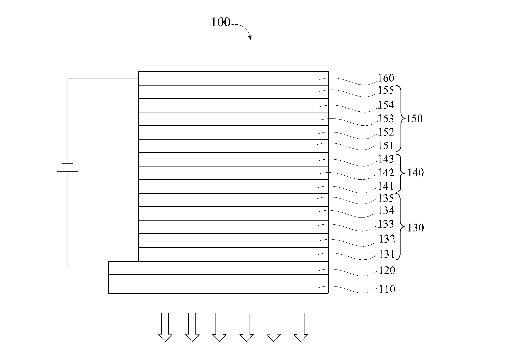
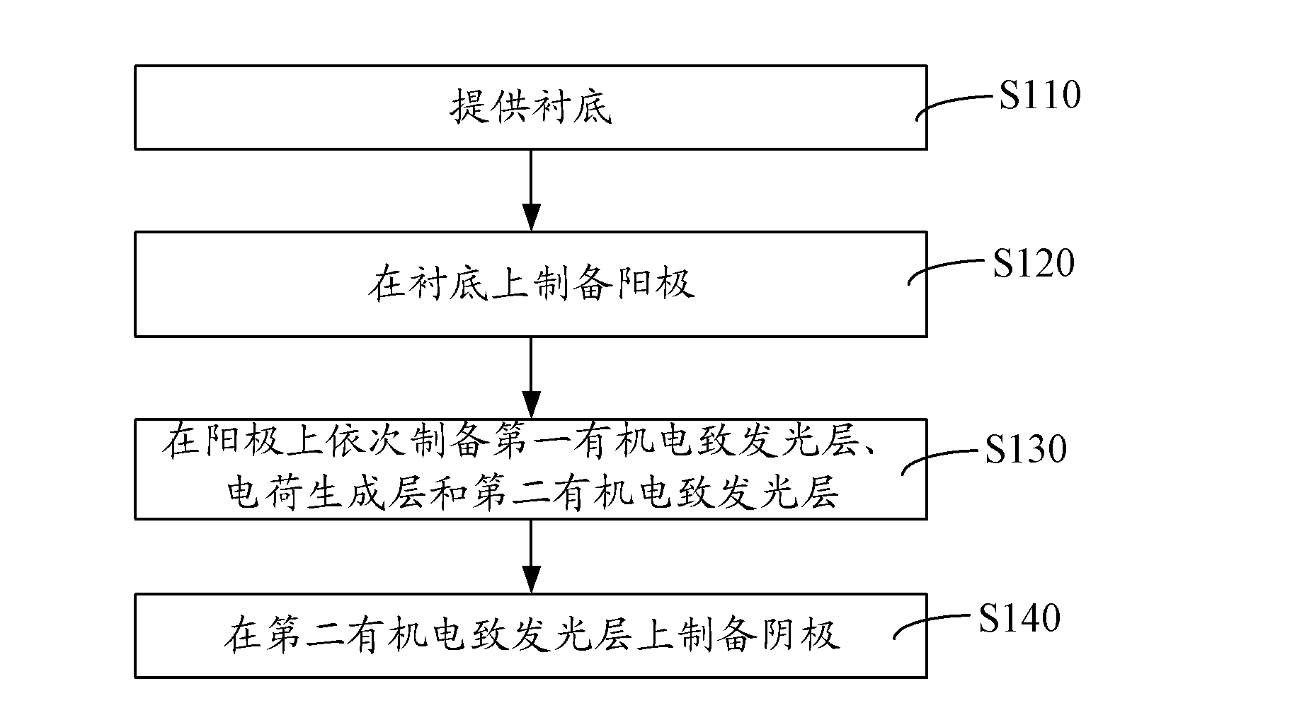
[0050] see figure 2 , the preparation method of the organic electroluminescence device of an embodiment, comprises the following steps:

[0051] Step S110: providing a substrate.

[0052] The substrate may be a glass substrate or a polyethersulfone resin substrate. After the substrate is washed, first place the substrate in deionized water containing detergent for ultrasonic cleaning, after cleaning, use ultrasonic treatment in isopropanol and acetone for 20 minutes, and then dry it with nitrogen to obtain a clean substrate. end.

[0053] Step S120: preparing an anode on the substrate in step S110.

[0054] In the vacuum coating system, a transparent conductive oxide or metal is evaporated, and a transparent conductive oxide film or a thin layer of metal is prepared on the substrate as an anode.

[0055] The transparent conductive oxide may be indium doped tin oxide (ITO), indium doped zinc oxide (IZO), aluminum doped zinc oxide (AZO) or gallium doped zinc oxide (GZO). T...
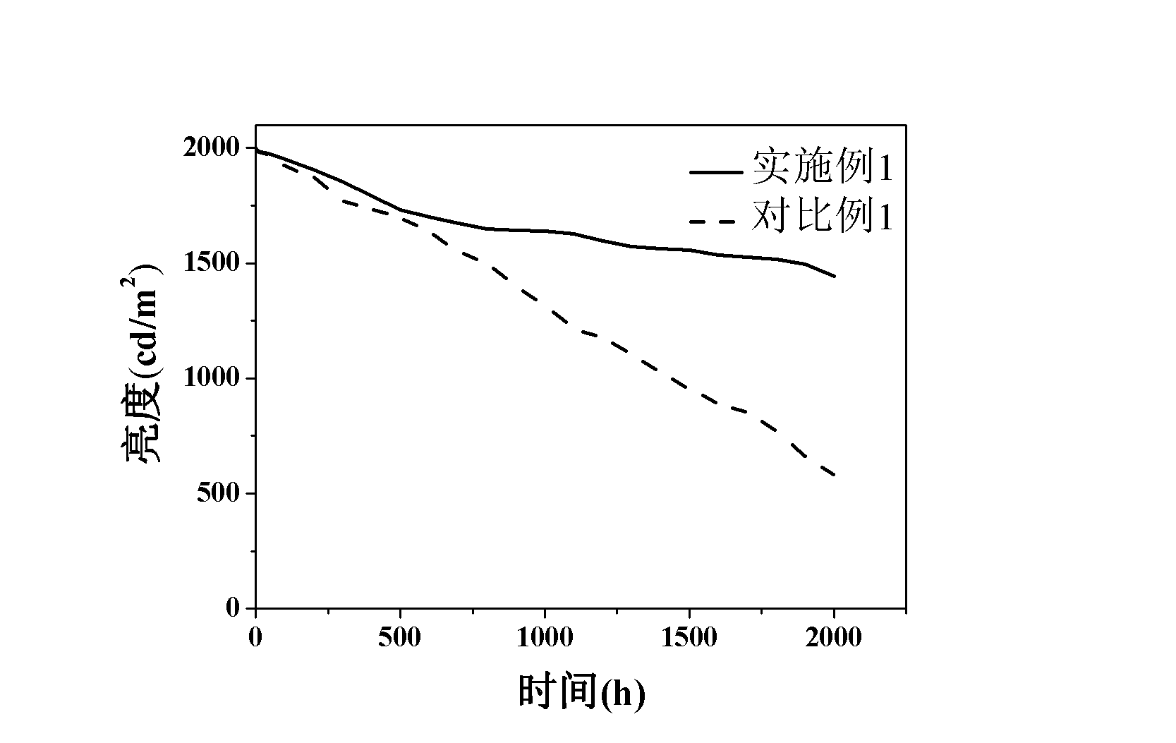
Embodiment 1

[0067] After the glass substrate is cleaned, in a vacuum sputtering system, an indium-doped tin oxide (ITO) film with a thickness of 100 nanometers is sputtered on its surface. After plasma treatment, it is then transferred to a vacuum thermal evaporation system. The first organic electroluminescence layer, the charge generation layer, the second organic electroluminescence layer and the cathode are sequentially evaporated on the surface of the ITO thin film.

[0068] The structure of the prepared first organic electroluminescent layer is:

[0069] m-MTDATA / NPB / Ir(ppy) 3 :CBP / Alq 3 / LiF.

[0070] The structure of the prepared second organic electroluminescent layer is:

[0071] m-MTDATA / NPB / Ir(ppy) 3 :CBP / Alq 3 / LiF.

[0072] The structure of the prepared charge generation layer is Mg / MoO 3 / Au, the thicknesses are 3 nm, 5 nm, and 15 nm, respectively.

[0073] The device structure is glass substrate / ITO / m-MTDATA / NPB / Ir(ppy) 3 :CBP / Alq 3 / LiF / Mg / MoO 3 / Au / m-MTDATA / NP...

Embodiment 2

[0075] After the glass substrate is cleaned, in a vacuum sputtering system, an indium-doped zinc oxide (IZO) film with a thickness of 120 nm is sputtered on its surface, and after plasma treatment, it is then transferred to a vacuum thermal evaporation system , vapor-depositing a first organic electroluminescent layer, a charge generation layer, a second organic electroluminescent layer and a cathode on the surface of the IZO thin film.

[0076] The structure of the prepared first organic electroluminescent layer is:

[0077] CuPc / TPD / FIrPic:CBP / TPBi / CsF.

[0078] The structure of the prepared second organic electroluminescent layer is:

[0079] m-MTDATA / TPD / (F-BT) 2 Ir(acac):CBP / TPBi / CsF.

[0080] The structure of the charge generation layer used is Yb / MoO 3 / Au, the thicknesses are 2 nm, 3 nm, and 10 nm, respectively.

[0081] The device structure is glass substrate / IZO / CuPc / TPD / FIrPic:CBP / TPBi / CsF / Yb / MoO 3 / Au / m-MTDATA / TPD / (F-BT) 2 Ir(acac):CBP / TPBi / CsF / Al.


PUM


Abstract

An organic electroluminescent device comprises a substrate, an anode, a first organic electroluminescent layer, a charge generating layer, a second organic electroluminescent layer and a cathode. The charge generating layer comprises a metal layer, a molybdenum oxide layer and a gold layer which are arranged on the first organic electroluminescent layer in a laminating mode. The metal layer is made of magnesium, aluminum, neodymium, samarium or ytterbium. The organic electroluminescent device is in a laminating structure; the charge generating layer is sequentially connected with the first organic electroluminescent layer and the second organic electroluminescent layer; and the charge generating layer comprises the metal layer, the molybdenum oxide layer and the gold layer which are arranged on the first organic electroluminescent layer in a laminating mode, so that the charge generating layer has the advantages of being high-efficiency in the charge generating property and rapid in the charge transmission property, generating more hole-electron luminous pairs, improving the luminous efficiency of the organic electroluminescent, increasing the current efficiency of the organic electroluminescent device in a multiplied mode along the number of luminous units which are in serious connection and being low in the driving current and high in the luminous efficiency.

Description

【Technical field】 [0001] The invention relates to the field of organic electroluminescent devices, in particular to an organic electroluminescent device and a preparation method thereof. 【Background technique】 [0002] Organic Light-Emitting Diode (Organic Light-Emitting Diode), hereinafter referred to as OLED, has the characteristics of high brightness, wide range of material selection, low driving voltage, fully cured active light emission, etc., and has high definition, wide viewing angle, and fast response speed, etc. The advantage is a display technology and light source with great potential, which conforms to the development trend of mobile communication and information display in the information age, and the requirements of green lighting technology. It is the focus of many researchers at home and abroad. [0003] Organic electroluminescent diodes have a sandwich-like structure, with a cathode and an anode at the top and bottom, and a single or multiple functional lay...

Claims


Application Information

Patent Timeline
Patent Type & Authority Applications(China)
IPC IPC(8): H01L51/50H01L51/56
Inventor 周明杰王平冯小明张振华
Owner OCEANS KING LIGHTING SCI&TECH CO LTD
Why Eureka
Try Eureka