OLED display device

A display device and display panel technology, which is applied to static indicators, instruments, etc., can solve problems such as discontinuous display gray scales, and achieve the effects of avoiding affecting the pixel aperture ratio, improving display uniformity, and ensuring continuity

Active Publication Date: 2018-03-16
SHENZHEN CHINA STAR OPTOELECTRONICS SEMICON DISPLAY TECH CO LTD
View PDF6 Cites 3 Cited by
  • Summary
  • Abstract
  • Description
  • Claims
  • Application Information

AI Technical Summary

Problems solved by technology

The switching switch K1' is controlled by the switching signal Switch', including the first pin K1', the second pin K2' and the third pin K3'; the gate of the first thin film transistor T1' is connected to the scan signal Scan', the drain is connected to the power supply voltage OVDD', the source is electrically connected to the gate of the second thin film transistor T2' and one end of the capacitor C1'; the drain of the second thin film transistor T2' is connected to the power supply voltage OVDD ', the source is electrically connected to the anode of the organic light emitting diode D1'; the cathode of the organic light emitting diode D1' is connected to the common ground voltage OVSS'; the other end of the capacitor C1' is electrically connected to the source of the second thin film transistor T2'; The gate of the three thin film transistor T3' is connected to the sensing control signal Sense', the source is electrically connected to the source of the second thin film transistor T2', and the drain is electrically connected to the first pin K1' of the switch K'; The second pin K2' of the switch K' is electrically connected to the digital-to-analog converter DAC', and the third pin K3' is electrically connected to the analog-to-digital converter ADC'. When the circuit charges the capacitor C1', it ensures organic light emission The diode D1' does not emit light, and the threshold voltage of the organic light emitting diode D1' needs to be limited to about 10V. The OLED device needs to be made into a triple stack device, which limits the number of layers of the OLED device, and when the organic light emitting diode D10 emits light, it is easy to appear the second thin film The difference between the gate-source voltage and the threshold voltage of the transistor T2' is greater than that of the source-drain voltage, so that the second thin film transistor T2' works in the linear region, displaying discontinuous gray scales, and flows through the power supply voltage OVDD' of the OLED device D1' The voltage drop (IRdrop) has a serious impact on

Method used


Image

  • OLED display device
  • OLED display device
  • OLED display device

Examples


Embodiment Construction

[0034] In order to further illustrate the technical means adopted by the present invention and its effects, the following describes in detail in conjunction with preferred embodiments of the present invention and accompanying drawings.

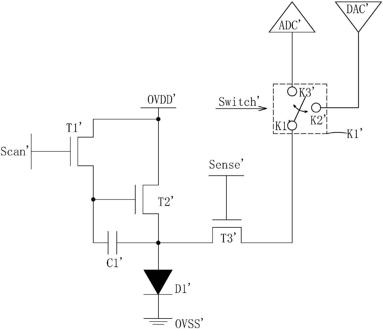
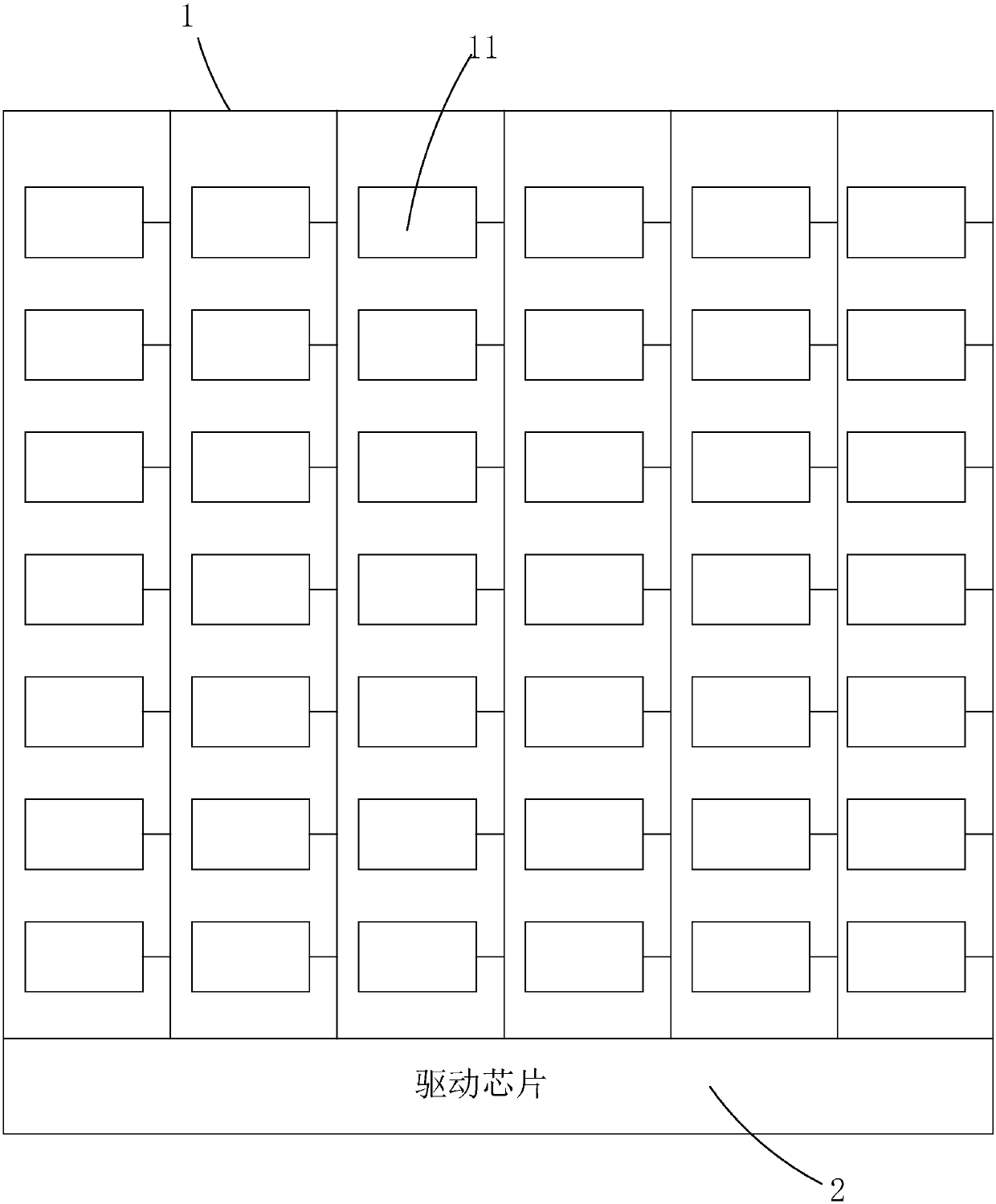
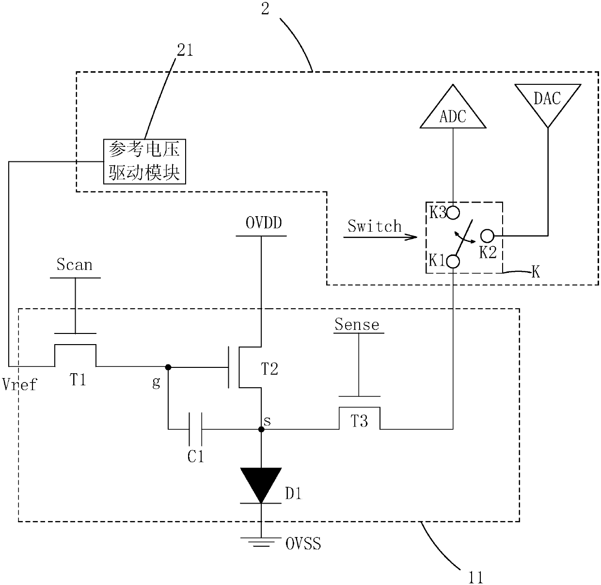
[0035] see figure 2 and image 3, the present invention provides an OLED display device, comprising: a display panel 1 and a drive chip 2 electrically connected to the display panel 1; the display panel 1 includes: a plurality of sub-pixels 11 arranged in an array; the drive chip 2 is provided with a switch K1, a digital-to-analog converter DAC, an analog-to-digital converter ADC, and a reference voltage drive module 21; the switch K is controlled by a switching signal Switch, including a first pin K1, a second pin K2 and The third pin K3; each sub-pixel 11 includes: a first thin film transistor T1, a second thin film transistor T2, a third thin film transistor T3, a capacitor C1 and an organic light emitting diode D1.

[0036] Wherein, the...


PUM


Abstract

The invention provides an OLED display device. According to the OLED display device, a 3T1C structure is employed for driving. A source of a first thin-film transistor is connected to a reference voltage; under control on the potential of the reference voltage, a second thin-film transistor works in a saturation region all the time when normal displaying is carried out to ensure continuity of thedisplay grayscales. Meanwhile, a reference voltage metal layer covering all sub pixels is used for replacing reference voltage routing to provide a reference voltage for the source of the first thin-film transistor, so that the influence on the pixel aperture ratio by the reference voltage routing is eliminated.

Description

technical field [0001] The invention relates to the field of display technology, in particular to an OLED display device. Background technique [0002] Organic light emitting diode (Organic Light Emitting Display, OLED) display device has self-illumination, low driving voltage, high luminous efficiency, short response time, high definition and contrast, nearly 180° viewing angle, wide operating temperature range, and can realize flexible display and With many advantages such as large-area full-color display, it is recognized by the industry as a display device with the most potential for development. [0003] The OLED is a current-driven device. When a current flows through the OLED, the OLED emits light, and the brightness of the light is determined by the current flowing through the OLED itself. Most existing integrated circuits (Integrated Circuit, IC) only transmit voltage signals, so the pixel driving circuit of the OLED needs to complete the task of converting the vol...

Claims


Application Information

Patent Timeline
Patent Type & Authority Applications(China)
IPC IPC(8): G09G3/3266
CPCG09G3/3266
Inventor 王振岭
Owner SHENZHEN CHINA STAR OPTOELECTRONICS SEMICON DISPLAY TECH CO LTD
Why Eureka
Try Eureka