Array substrate, manufacturing method of array substrate and display device

A technology of an array substrate and a manufacturing method, which is applied in the display field, can solve problems such as influence and large data line load, and achieve the effect of reducing load and reducing the front area

Active Publication Date: 2015-10-07
CHONGQING BOE OPTOELECTRONICS +1
View PDF5 Cites 16 Cited by
  • Summary
  • Abstract
  • Description
  • Claims
  • Application Information

AI Technical Summary

Problems solved by technology

[0005] In order to solve the problem that the signal of the shielding electrode affects the signal on the data line, resulting in a large load on the data line, the present invention provides an array substrate, a manufacturing method thereof, and a display device

Method used


Image

  • Array substrate, manufacturing method of array substrate and display device
  • Array substrate, manufacturing method of array substrate and display device
  • Array substrate, manufacturing method of array substrate and display device

Examples


Embodiment Construction

[0098] In order to make the object, technical solution and advantages of the present invention clearer, the present invention will be further described in detail below in conjunction with the accompanying drawings. Obviously, the described embodiments are only some embodiments of the present invention, rather than all embodiments . Based on the embodiments of the present invention, all other embodiments obtained by persons of ordinary skill in the art without making creative efforts belong to the protection scope of the present invention.

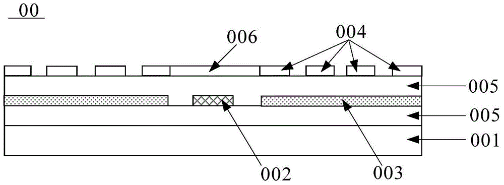
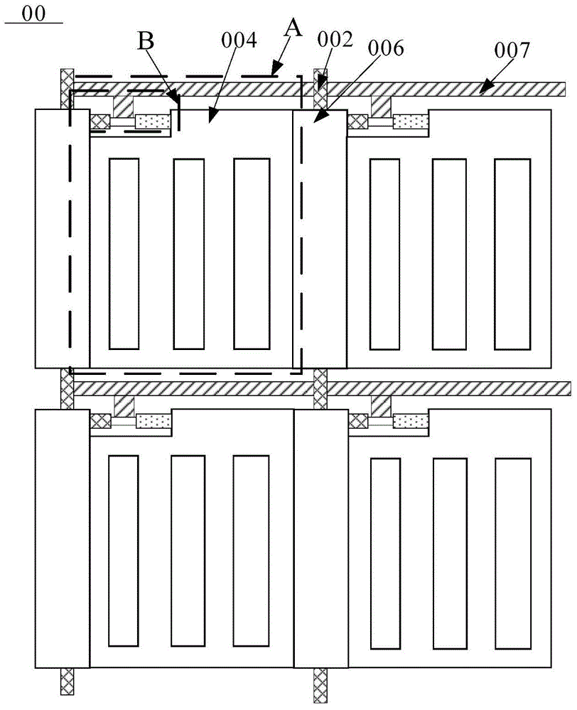
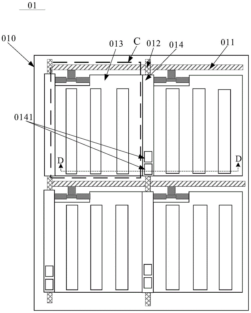
[0099] Please refer to figure 2 , which shows a top view of the array substrate 00 provided by the related art, see figure 2 , the array substrate 00 includes a base substrate ( figure 2 not shown in ), and a plurality of gate lines 007 ( figure 2 Only draw two) and data line 002 ( figure 2 Only two of them are drawn), each data line 002 and gate line 007 intersect and are insulated, and the adjacent two data lines 002 and the adja...


PUM


Abstract

The invention discloses an array substrate, a manufacturing method of the array substrate and a display device, and belongs to the technical field of display. The array substrate comprises a substrate body. A data line is formed on the substrate body. A first electrode is formed on the substrate body on which the data line is formed. A first insulating layer is formed on the substrate body on which the first electrode is formed. A second electrode and a guard electrode are formed on the substrate body on which the first insulating layer is formed. The orthographic projection of the data line on the substrate body falls into the orthographic projection of the guard electrode on the substrate body. At least one opening is formed in the guard electrode, and the openings are located in the orthographic projection area of the data line on the guard electrode. The openings are formed in the guard electrode, the problem that signals of the guard electrode have an effect on signals of the data line, and consequently the load of the data line is large is solved, and the effect of reducing the load of the data line is achieved.

Description

technical field [0001] The present invention relates to the field of display technology, in particular to an array substrate, a manufacturing method thereof, and a display device. Background technique [0002] With the continuous development of display technology, display devices are widely used in the field of display. Existing display devices can generally be Thin Film Transistor Liquid Crystal Displays (English: Thin Film Transistor Liquid Crystal Display, referred to as TFT-LCD). TFT-LCD is known for its Large size, highly integrated, powerful, flexible process, low cost and other advantages are widely used in televisions, computers, mobile phones and other fields. [0003] A display device may generally include an array substrate and a color filter substrate formed in a cell, and a liquid crystal layer filled between the array substrate and the color filter substrate. figure 1 It is a schematic structural diagram of an array substrate 00 provided in the related art, se...

Claims


Application Information

Patent Timeline
Patent Type & Authority Applications(China)
IPC IPC(8): G02F1/1362G02F1/1368G02F1/1343
CPCG02F1/134309G02F1/136286G02F1/1368G02F1/136218G02F1/136295
Inventor 齐智坚陈帅顾可可杨妮胡伟
Owner CHONGQING BOE OPTOELECTRONICS
Why Eureka
Try Eureka