Wafer soaking device

A technology of wafers and wafers, which is applied in the field of wafer wet processing in the semiconductor industry, can solve the problems of uniform waiting time, and achieve the effects of simple structure, easy observation, and reduced volatilization and environmental impact

Active Publication Date: 2015-10-14
SHENYANG KINGSEMI CO LTD
View PDF5 Cites 5 Cited by
  • Summary
  • Abstract
  • Description
  • Claims
  • Application Information

AI Technical Summary

Problems solved by technology

[0003] In order to solve the uniformity of the soaking time of a single wafer and the waiting time after taking it out during the wafer soaking process, the main purpose of the present invention is to provide a wafer soaking device that can transfer wafers in time-sharing and meet higher requirements for wafer soaking

Method used


Image

  • Wafer soaking device
  • Wafer soaking device
  • Wafer soaking device

Examples


Embodiment Construction

[0023] The present invention will be described in further detail below in conjunction with the accompanying drawings.

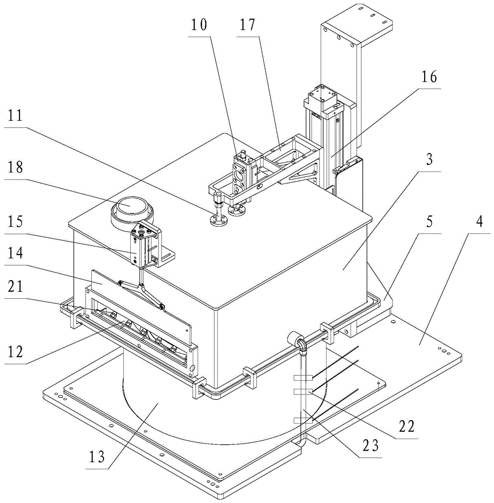
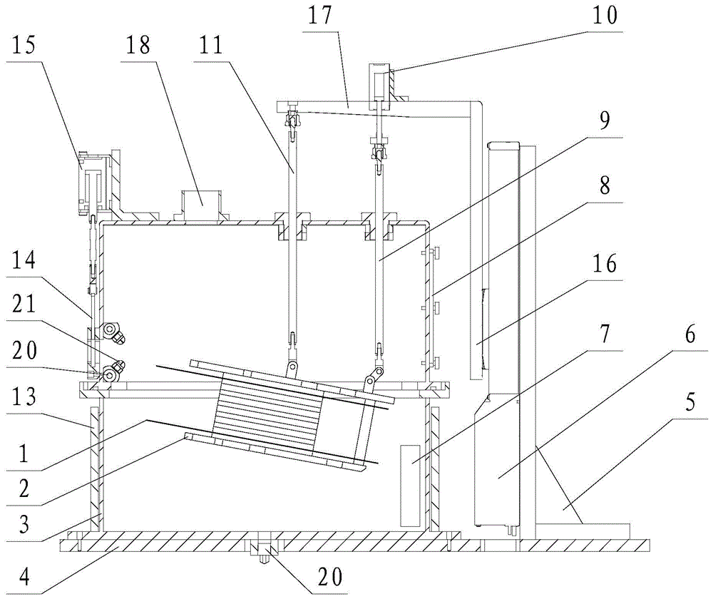
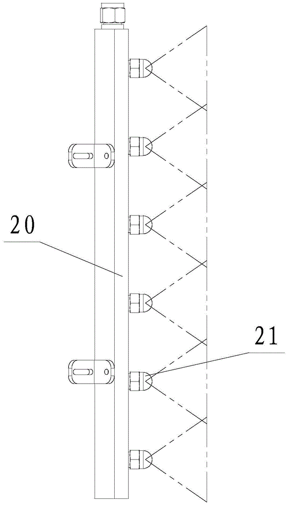
[0024] Such as figure 1 , figure 2 As shown, the present invention includes a film box 2, a liquid storage tank 3, a base plate 4, a support 5, an electric actuator 6, an ultrasonic generator 7, an inclined connecting rod 9, an inclined cylinder 10, a lifting connecting rod 11, a film transfer window 12, Heating plate 13, baffle plate 14, lifting cylinder 15, mounting plate 16, connecting plate 17, air blowing pipe 20 and air nozzle 21, wherein the liquid storage tank 3 is fixed on the bottom plate 4, is a closed cavity, the upper part of the liquid storage tank 3 It is a cuboid or cube, and the lower part is barrel-shaped; the electric actuator 6 is fixed on the bottom plate 4 through the bracket 5, and is located on one side of the liquid storage tank 3. The chip box 2 is located in the liquid storage tank 3, and multiple chips 1 can be loaded in the chi...


PUM


Abstract

The invention belongs to the technical field of wafer wet processing in the semiconductor industry and specifically relates to a wafer soaking device which meets wafer soaking requirements. A liquid storage tank and an electric actuator are arranged on a bottom board; a wafer box is arranged in the liquid storage tank; one end of a lifting connection rod is connected with the output end of the electric actuator, and the other end is inserted into the liquid storage tank and is hinged with the wafer box; the tank groove of the upper portion of the liquid storage tank is provided with a wafer feeding window for allowing a mechanical arm to feed the wafers into the wafer box; the electric actuator drives the lifting connection rod to drive the wafer box to go up and down, so that the wafer box is allowed to rise to the height corresponding to the wafer feeding window to facilitate to fetch and release the wafers, or the wafer box is allowed to decline and be immersed into chemical liquid for soaking the wafers; the inner upper and lower two sides of the wafer feeding window are respectively provided with an air blowpipe arranged on the liquid storage tank; the air blowpipes are communicated with an air source; and each air blowpipe is uniformly provided with a plurality of air mouths. The wafer soaking device realizes uniformity of soaking time of each signal wafer and waiting time after the wafer is taken out, and realizes higher requirements for wafer soaking in the wet processing process.

Description

technical field [0001] The invention belongs to the field of wafer wet processing in the semiconductor industry, in particular to a wafer soaking device meeting the wafer soaking requirements. Background technique [0002] At present, the wafer wet processing process in the semiconductor industry often requires the use of chemical liquid to soak the wafer. The current wafer soaking method generally uses the whole box of wafers to be soaked in the chemical liquid tank at the same time, and then the whole box is taken out for the next process after the predetermined time; The wafers are processed sequentially, which results in a different waiting time for each piece of the whole box of wafers, which may affect the quality of the final chip. Therefore, how to achieve the uniformity of soaking time for each wafer is an inevitable problem. Contents of the invention [0003] In order to solve the uniformity of the soaking time of a single wafer and the waiting time after takin...

Claims


Application Information

Patent Timeline
Patent Type & Authority Applications(China)
IPC IPC(8): H01L21/67
Inventor 谷德君王一
Owner SHENYANG KINGSEMI CO LTD
Why Eureka
Try Eureka