Touch display panel and manufacturing method and driving method thereof and display device

A touch display panel and touch technology are applied in the field of driving methods and display devices, touch display panels, and manufacturing methods thereof, and can solve the problems of touch signal display signal interference, limited touch driving frequency, large coupling capacitance, etc. question

Active Publication Date: 2015-10-21
BOE TECH GRP CO LTD +1
View PDF3 Cites 18 Cited by
  • Summary
  • Abstract
  • Description
  • Claims
  • Application Information

AI Technical Summary

Problems solved by technology

And in the small size touch screen, such as figure 1 As shown, in the touch stage, the common electrodes are multiplexed as touch self-capacitance electrodes 001, and each touch self-capacitance electrode 001 is connected to the touch chip through the touch lead 002. The overlapping area between the lines and the data lines is large, resulting in a large coupling capacitance, causing interference of the touch signal to the display signal, and limiting the touch driving frequency

Method used


Image

  • Touch display panel and manufacturing method and driving method thereof and display device
  • Touch display panel and manufacturing method and driving method thereof and display device
  • Touch display panel and manufacturing method and driving method thereof and display device

Examples


Embodiment Construction

[0041] The specific implementation manners of the touch display panel provided by the embodiments of the present invention, its manufacturing method, driving method and display device will be described in detail below with reference to the accompanying drawings.

[0042] Wherein, the thickness and shape of each film layer in the drawings do not reflect the real scale of the touch display panel, and the purpose is only to illustrate the content of the present invention.

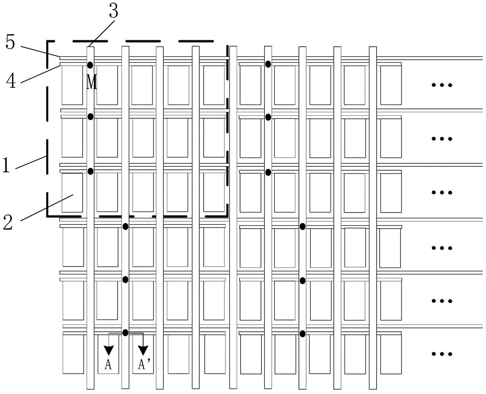
[0043] An embodiment of the present invention provides a touch display panel, such as figure 2 As shown, it includes: an array substrate, and a plurality of pixel units arranged in a matrix are arranged in the array substrate; wherein,

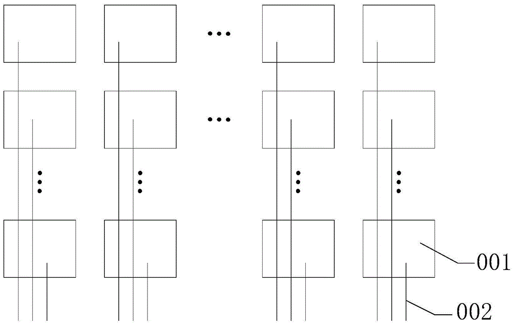
[0044] The array substrate also includes a plurality of touch self-capacitance electrodes 1, which are arranged in a matrix, and each touch self-capacitance electrode 1 includes a plurality of electrode blocks 2, and each electrode block 2 corresponds to a pixel unit one by o...


PUM


Abstract

The invention discloses a touch display panel and a manufacturing method and driving method thereof and a display device. According to the touch display panel, a plurality of pixel units are arranged in an array substrate in a matrix mode; the array substrate comprises a plurality of touch self-capacitance electrodes arranged in a matrix mode, and each touch self-capacitance electrode comprises a plurality of electrode blocks corresponding to the pixel units one to one; the array substrate further comprises touch leads corresponding to the touch self-capacitance electrodes one to one, the touch leads are arranged in clearances between the adjacent pixel units corresponding to the touch self-capacitance electrodes, and the touch self-capacitance electrodes are connected with touch chips through the touch leads. Due to the fact that the electrode blocks correspond to the pixel units one to one and are arranged in areas defined by adjacent grid lines and data lines, the electrode blocks are not overlapped with the grid lines or the data lines, coupling capacitance between the electrode blocks and the grid lines and between the electrode blocks and the data lines is lowered, loads are reduced, touch sensitivity is improved, and the excellent touch performance of the large-size display panel is achieved.

Description

technical field [0001] The invention relates to the field of display technology, in particular to a touch display panel, a manufacturing method, a driving method and a display device. Background technique [0002] At present, with the development of display technology, display technology is widely used in TV, mobile phone and display of public information. Screen Panel) has gradually pervaded people's lives. Today, in the pursuit of excellent experience functions, touch performance has always been a major defect of large-size display panels, either limited by technology or limited by cost. [0003] At present, there are mainly three types of embedded touch panels: resistive touch panels, capacitive touch panels, and optical touch panels. The corresponding embedded touch technology has been initially applied to small-size displays. Excellent touch performance has become the direction of future touch design, and therefore, it also provides a direction for efforts to realize t...

Claims


Application Information

Patent Timeline
Patent Type & Authority Applications(China)
IPC IPC(8): G06F3/044
CPCG06F3/0412G06F3/04164G06F3/04166G06F3/0443G06F2203/04103G06F2203/04107G06F2203/04111
Inventor 丁小梁董学王海生陈小川赵卫杰杨盛际刘伟刘英明刘红娟王磊李昌峰许睿
Owner BOE TECH GRP CO LTD
Why Eureka
Try Eureka