
Reading circuit of non-volatile memory capable of preventing side channel attack

A memory read and bypass attack technology, applied in static memory, read-only memory, information storage, etc., can solve problems such as read bypass signal leakage, unacceptable array area, and extended read time

Active Publication Date: 2015-11-04
FUDAN UNIV
View PDF3 Cites 14 Cited by
  • Summary
  • Abstract
  • Description
  • Claims
  • Application Information

AI Technical Summary

Problems solved by technology

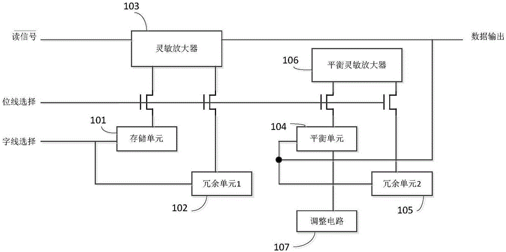
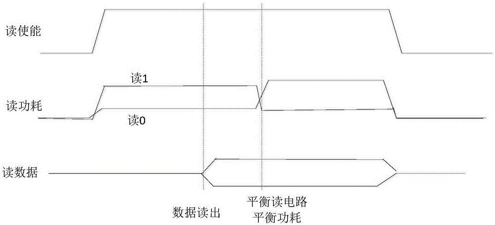
[0006] from figure 2 It can be seen that the problem with this technology is that after the data is read normally, the structure starts a read operation of a balanced read module according to the read data to balance the total read energy consumption. : First, the total reading time is extended to twice the time, and second, the structure essentially balances the reading energy consumption, while the instant power consumption curves of reading 0 and reading 1 are completely different, which will also become a read bypass signal Leaked sources, opening up opportunities for side channel attackers
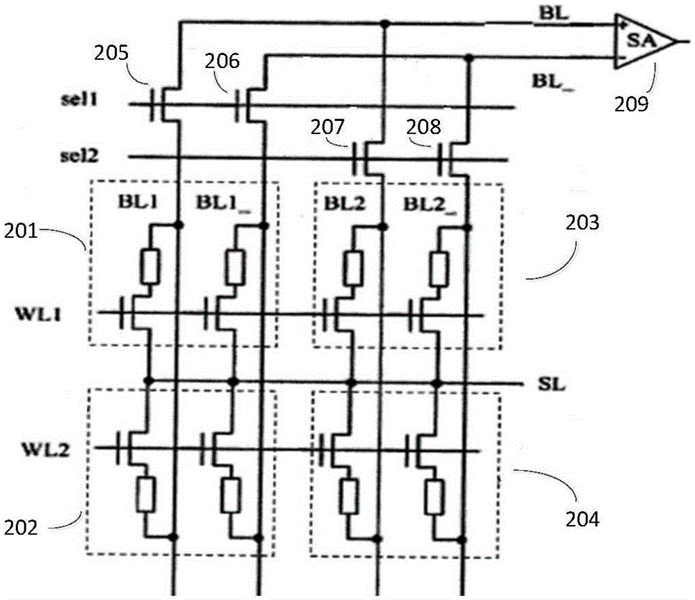
The disadvantage of this structure is that each storage bit contains two storage units, which doubles the array area, which is acceptable for small-capacity applications, but for slightly larger-capacity applications, the increase in the array area will be unacceptable

Method used


Image

  • Reading circuit of non-volatile memory capable of preventing side channel attack
  • Reading circuit of non-volatile memory capable of preventing side channel attack
  • Reading circuit of non-volatile memory capable of preventing side channel attack

Examples


Embodiment Construction

[0063] The specific implementation of the present invention will be further described in detail below in conjunction with the examples.

[0064] Figure 7 is based on Figure 4 A specific embodiment of the first circuit structure proposed by the present invention is shown, taking a resistive memory as an example, and focusing on an implementation of a voltage difference amplifier circuit. Figure 7 Among them, the storage unit 701 is a 1T1R unit composed of a transistor and a resistive unit R connected in series, and the reference unit 702 in the on state is a reference unit composed of a transistor connected in series with a resistive unit RL preset to low resistance. Unit, the reference unit 703 in the non-conducting state is a reference unit composed of a transistor connected in series with a resistive switching unit RH preset to high resistance.

[0065] The voltage difference amplifying circuit 707 includes an inverter Inv1 721 whose inversion voltage is specially adjus...


PUM


Abstract

The invention belongs to the technical field of a semiconductor memory, and particularly relates to a reading circuit structure of a non-volatile memory capable of preventing side channel attack. The structure comprises a storage unit, a first reference unit, a second reference unit, a voltage difference amplification circuit, a sensitivity amplifier, a current source, a column selection transistor, two reference unit column selection transistors, two reading enabling control transistors and two gates, wherein the storage unit is in a conduction state or non-conduction state; the conduction state represents 1 data storage; the non-conduction state represents 0 data storage; the first reference unit and the second reference unit have the same structure as the storage unit; the first reference unit is pre-programmed into the non-conduction state; and the second reference unit is pre-programmed into the conduction state. In the structure, a path of complementary reference unit columns can be opened at the same time in the reading process, so that a reading power consumption curve is balanced; therefore the side channel attack of the power consumption analysis can be prevented. According to another circuit structure, on the basis of the structure, the reference units in a middle state are used for performing reading operation; the reference units are used as redundancy units for balancing the reading power consumption; a 0 reading power consumption curve and a 1 reading power consumption curve can be further balanced; and the resistance on the power consumption analysis type side channel attack is facilitated.

Description

technical field [0001] The invention belongs to the technical field of semiconductor memory, and in particular relates to a non-volatile memory read circuit, in particular to a non-volatile memory read circuit capable of resisting bypass attacks to steal data. Background technique [0002] In the information age, while information technology provides convenience to people, it also brings a serious problem, that is, information security, especially the security of sensitive data. [0003] Although in the field of information security research, many technologies have been proposed for the algorithm layer and encryption circuit layer of security encryption, from the perspective of sensitive data storage, if the memory generates various leaked information during read and write operations, these The information is called side channel information, and it can also allow an attacker to discover the sensitive data stored in it. This type of attack is a side-channel attack. The prere...

Claims


Application Information

Patent Timeline
IPC IPC(8): G11C16/26
Inventor 解玉凤金越林殷茵
Owner FUDAN UNIV
Learn More